Light-emitting diode device and method for manufacturing the same
- Summary
- Abstract
- Description
- Claims
- Application Information
AI Technical Summary
Benefits of technology
Problems solved by technology
Method used
Image

Examples
first embodiment
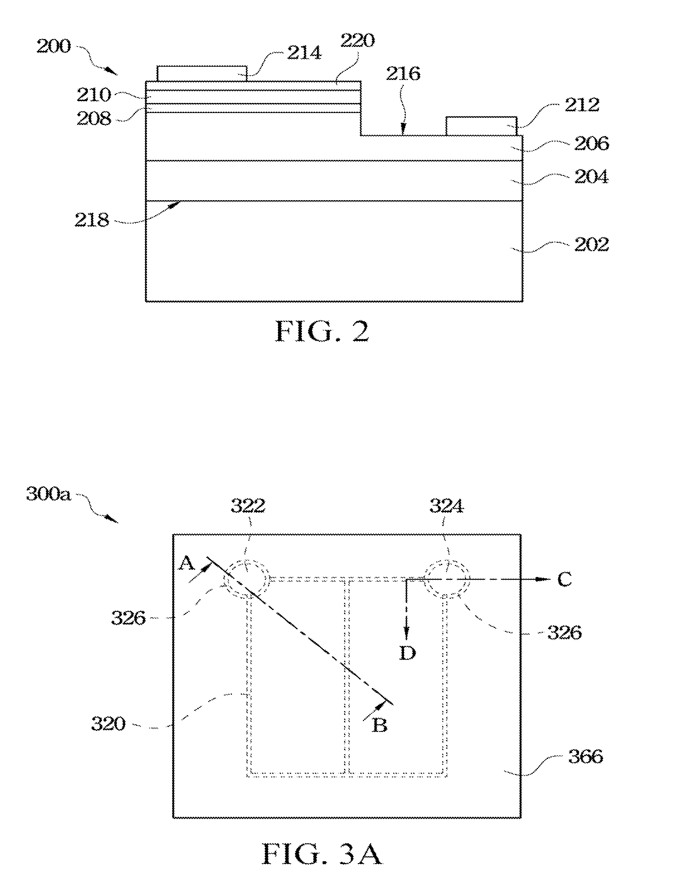
[0046]Referring to FIG. 3A to FIG. 3C, FIG. 3A is a top view of an LED device according to the present invention, FIG. 3B is a cross-sectional view taken along a cross-sectional line A-B in FIG. 3A and FIG. 3C is a cross-sectional view taken along a cross-sectional line C-D in FIG. 3A. In this embodiment, an LED device 300a mainly includes a substrate 302, a bonding layer 304, an epitaxial structure 328, a first electrical type conductive branch 320, a first electrical type electrode layer 322, an insulating layer 326 and a second electrical type electrode layer 338, as shown in FIG. 3B.
[0047]In the LED device 300a, the substrate 302 has surfaces 334 and 336 respectively located on two opposite sides thereof. The epitaxial structure 328 is bonded to the surface 334 of the substrate 302 by the bonding layer 304, that is, the bonding layer 304 is bonded between the epitaxial structure 328 and the surface 334 of the substrate 302. The material of the bonding layer 304 is a conductive m...
second embodiment
[0069]In the present invention, the first electrical type electrode layer and the second electrical type electrode layer may be located on the same plane. Referring to FIG. 5A and FIG. 5B, FIG. 5A is a top view of an LED device according to the present invention and FIG. 5B is a cross-sectional view taken along a cross-sectional line E-F in FIG. 5A. In this embodiment, the architecture of an LED device 300b is substantially the same as that of the LED device 300a of the above embodiment, and the difference lies in that the epitaxial structure 328 of the LED device 300b further includes another groove 344 penetrating the epitaxial structure 328, as shown in FIG. 5B. Secondly, the second electrical type electrode layer 346 of the LED device 300b is located in the groove 344, and the second electrical type electrode layer 346 is electrically connected to the second electrical type semiconductor layer 308 through the conductive layer 350. Additionally, the second electrical type electro...
third embodiment
[0083]FIG. 7A and FIG. 7B are cross-sectional views of processes of an LED device according to the present invention. In this embodiment, when the LED device 300c as shown in FIG. 7B is fabricated, similar to the description of the above embodiment with reference to FIG. 4A to FIG. 4D, a plurality of the epitaxial chips as shown in FIG. 4D may be formed on the wafer. Then, the epitaxial chips formed on the wafer are cut and separated.
[0084]Afterwards, a substrate 354 is provided. The substrate 354 may be for example a package substrate, a highly thermally conductive substrate or a package frame. Then, for example, a deposition process is employed to form the bonding layer 356 covering the surface of the substrate 354. The material of the bonding layer 356 may be a conductive material, e.g. Au, AuSn or In. In one embodiment, the bonding layer 356 may be used as the second electrical type electrode layer of the LED device 300c. In another embodiment, a second electrical type electrode...
PUM
 Abstract
Description
Claims
Application Information
 - Generate Ideas
- Intellectual Property
- Life Sciences
- Materials
- Tech Scout
- Unparalleled Data Quality
- Higher Quality Content
- 60% Fewer Hallucinations
Browse by: Latest US Patents, China's latest patents, Technical Efficacy Thesaurus, Application Domain, Technology Topic, Popular Technical Reports.
© 2025 PatSnap. All rights reserved.Legal|Privacy policy|Modern Slavery Act Transparency Statement|Sitemap|About US| Contact US: help@patsnap.com