Pixel array substrate and display panel

a technology of pixel array and substrate, applied in the direction of discharge tube luminescnet screen, coupling device connection, instruments, etc., can solve the problem of large resistance value differences in conventional techniques that do not occur, and achieve the effect of reducing the resistance difference of each trace to the corresponding signal line and ameliorating the problem of bright and dark lines

Inactive Publication Date: 2012-12-06
CHUNGHWA PICTURE TUBES LTD
View PDF5 Cites 9 Cited by
  • Summary
  • Abstract
  • Description
  • Claims
  • Application Information

AI Technical Summary

Benefits of technology

[0025]In the pixel array substrate and the display panel according to embodiments of the invention, the traces disposed in the periphery circuit region and belonging to different layers are connected to the signal lines in the display region by the conductive structures. Therefore, a resistance difference of each trace to the corresponding signal lines can be effectively lowered, thereby ameliorating the issue of bright and dark lines caused by differences in resistance values in conventional techniques.

Problems solved by technology

The issue of bright and dark lines caused by large differences in resistance values in conventional techniques does not occur easily in the display panel.

Method used


Image

  • Pixel array substrate and display panel
  • Pixel array substrate and display panel
  • Pixel array substrate and display panel

Examples


first embodiment

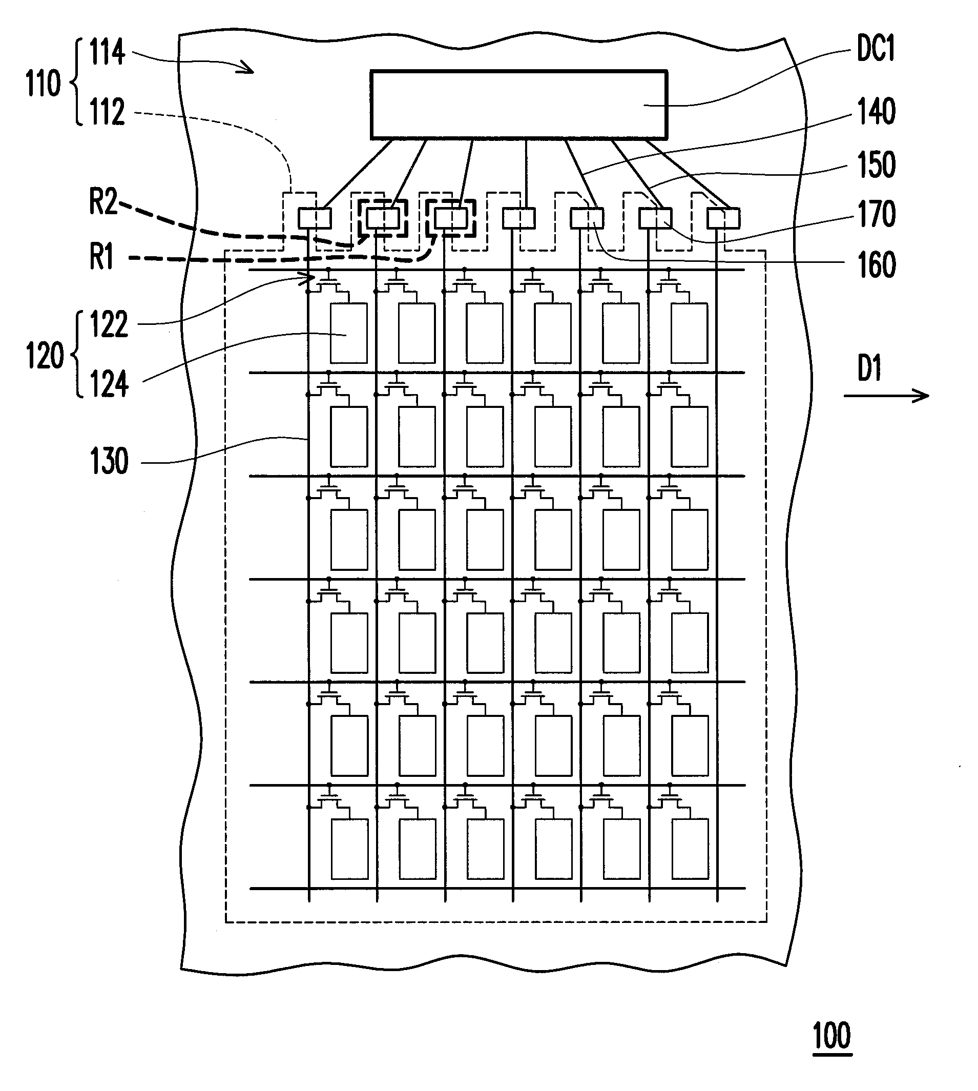
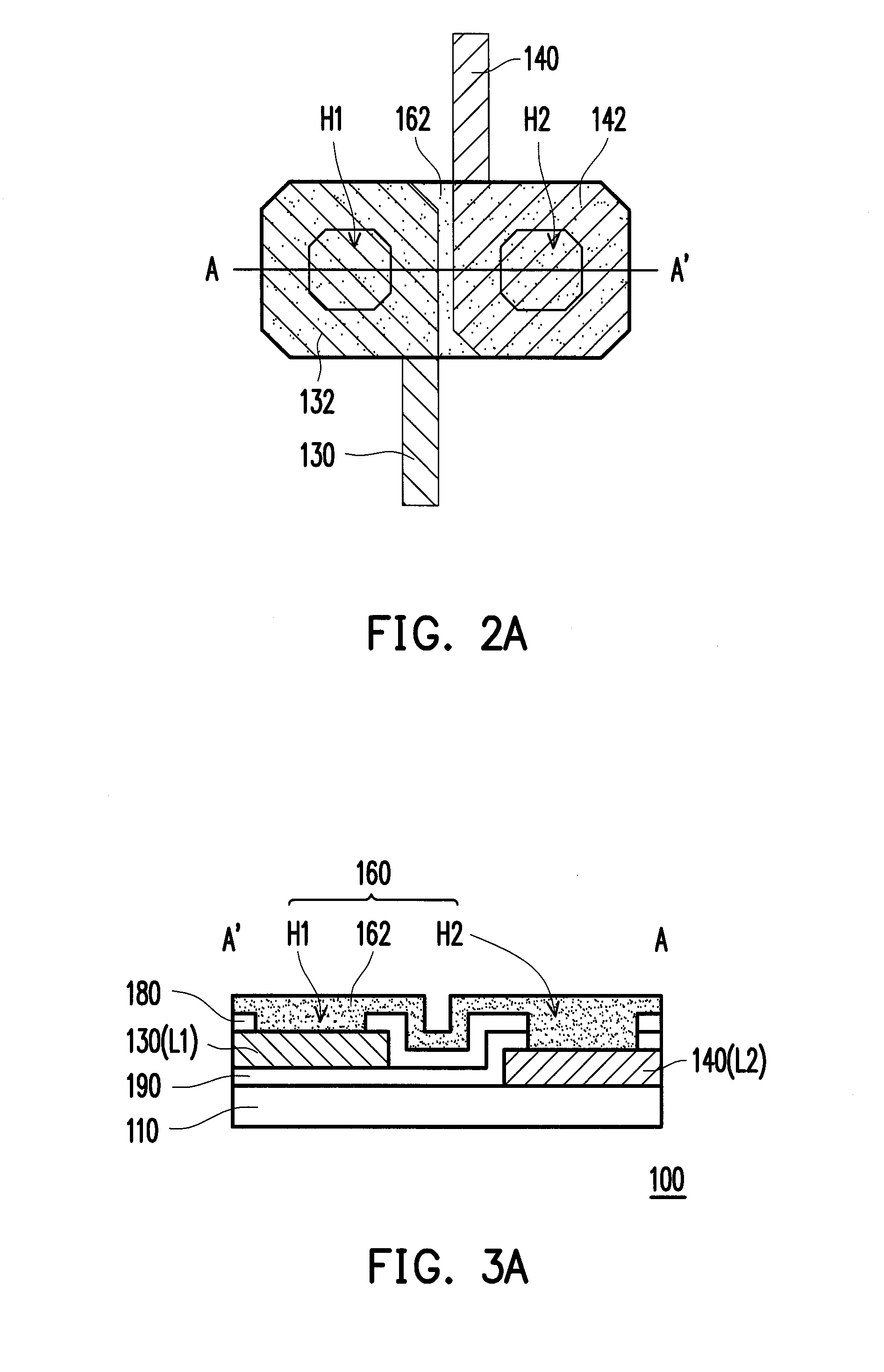
[0038]FIG. 1 is a schematic top view of a pixel array substrate according to an embodiment of the invention. Referring to FIG. 1, a pixel array substrate 100 of the present embodiment includes a substrate 110, a plurality of pixel structures 120, a plurality of signal lines 130, a plurality of first traces 140, a plurality of second traces 150, a plurality of first conductive structures 160, and a plurality of second conductive structures 170.

[0039]The substrate 110 of the present embodiment includes a display region 112 and a periphery circuit region 114. The periphery circuit region 114 is substantially connected to the display region 112. In the present embodiment, the substrate 110 is used for element carriage, and a material thereof may be glass, quartz, organic polymer, opaque / reflective material (e.g., a conductive material, a wafer, a ceramic material), or other suitable materials.

[0040]The pixel structures 120 of the present embodiment are arranged in array in the display r...

second embodiment

[0052]FIG. 5 is a schematic top view of a pixel array substrate according to an embodiment of the invention. With reference to FIG. 5, a pixel array substrate 500 of the present embodiment and the pixel array substrate 100 of the first embodiment are similar, and a difference therebetween mainly lies in that the signal lines 530 of the present embodiment are scan lines, and a drive circuit DC2 is correspondingly a gate driver. The pixel array substrate 500 of the present embodiment includes a substrate 510, a plurality of pixel structures 120, a plurality of signal lines 530, a plurality of first traces 540, a plurality of second traces 550, a plurality of first conductive structures 560, and a plurality of second conductive structures 570.

[0053]The substrate 510 of the present embodiment includes a display region 512 and a periphery circuit region 514. The periphery circuit region 514 is substantially connected to the display region 512. The pixel structures 120 of the present embo...


PUM


Abstract

A pixel array substrate includes a substrate, a plurality of pixel structures, a plurality of signal lines, a plurality of first traces, a plurality of second traces, a plurality of first conductive structures, and a plurality of second conductive structures. The pixel structures are arranged in array in a display region of the substrate. The signal lines are disposed in the display region and are formed in a first conducting wire layer and are electrically connected to the pixel structures. The first traces and the second traces are disposed in a periphery circuit region of the substrate and are respectively formed in a second conducting wire layer and the first conducting wire layer. A part of the signal lines are electrically connected to the first traces by the first conductive structures. Another of the signal lines are electrically connected to the second traces by the second conductive structures.

Description

CROSS-REFERENCE TO RELATED APPLICATION[0001]This application claims the priority benefit of Taiwan application serial no. 100209945, filed on Jun. 1, 2011. The entirety of the above-mentioned patent application is hereby incorporated by reference herein and made a part of this specification.BACKGROUND OF THE INVENTION[0002]1. Field of Invention[0003]The invention relates to a pixel array substrate and a display panel, and more particularly to a pixel array substrate and a display panel having a dual trace.[0004]2. Description of Related Art[0005]With the vigorous development of display technologies, display panels have been applied in display devices of various dimensions, such as televisions, computer monitors, notebook computers, mobile phones, etc. Taking televisions for example, the consumer not only has demands in display properties such as resolution, contrast, and viewing angle, but the consumer is also increasingly making exterior aesthetics a deciding factor for purchase. T...

Claims


Application Information

Patent Timeline
Patent Type & Authority Applications(United States)
IPC IPC(8): H01J1/62H05K1/18
CPCG02F1/13454G02F1/1345
Inventor ZENG, GUANG-YITSAI, YI-CHENG
Owner CHUNGHWA PICTURE TUBES LTD
Why Eureka
Try Eureka