Scintillator plate

US20120313013A1Inactive Publication Date: 2012-12-13SIEMENS AG
1 Cites 2 Cited by

Patent Information

Authority / Receiving Office
US · United States
Current Assignee / Owner
Publication Date
2012-12-13
Estimated Expiration
Not applicable · inactive patent

Smart Images

  • Figure 1
    Figure 1
Patent Text Reader

Abstract

A scintillator plate has a radiation-permeable substrate on which is applied a scintillator layer made of copper iodide that is formed from spicular crystals. The scintillator layer has an emission maximum in the red spectral range. The scintillator layer of the scintillator plate has a high emission power in the near-infrared range.
Need to check novelty before this filing date? Find Prior Art

Description

BACKGROUND OF THE INVENTION

[0001] 1. Field of the Invention

[0002] The invention concerns a scintillator plate with a radiation-permeable substrate on which is applied a scintillator layer formed from spicular (needle-shaped) crystals.

[0003] 2. Description of the Prior Art

[0004] A scintillator plate of the above type is used, for example, in a digital x-ray detector (flat panel detector) in combination with an active matrix (two-dimensional, pixelated photosensor) that is subdivided into a plurality of pixel readout units with photosensors. The incident x-ray radiation is initially converted in the scintillator layer of the scintillator plate into visible light that is subsequently transduced by the photosensors into electrical charge and is stored with spatial resolution. This conversion (known as an indirect conversion) is described in the article by M. Spahn et al. “Flachbilddetektoren in der Röntgendiagnostik” [“Flat panel detectors in x-ray diagnostics”] in “Der Radiologe [The Radio...

Examples

Embodiment Construction

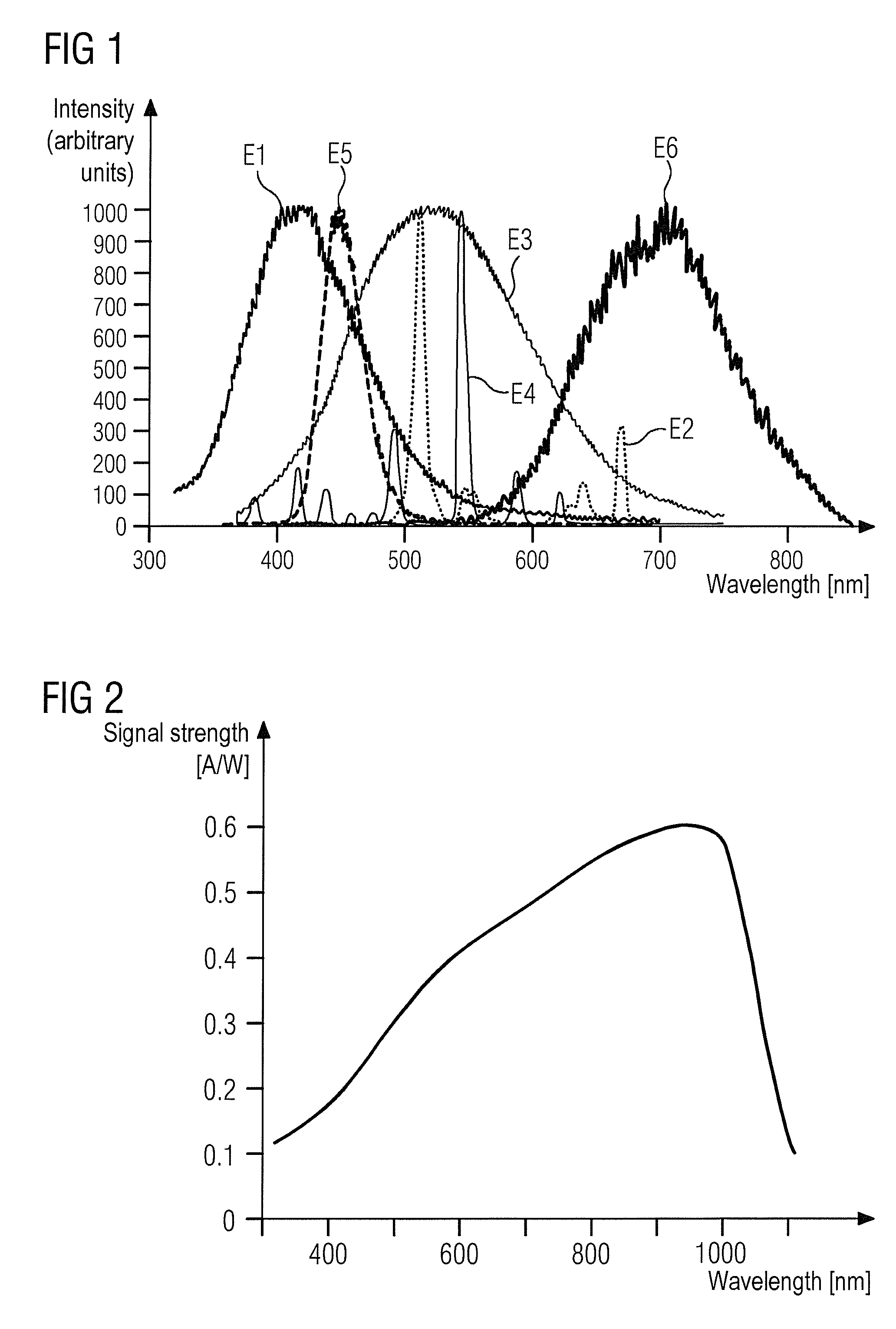
[0023]The emission spectra E1 through E4 of the following scintillator materials according to the prior art are shown in FIG. 1:

[0024]E1 CsI:Na (cesium iodide, doped with sodium) with an emission maximum at approximately 420 nm,

[0025]E2 Gd2O2S:Pr,Ce (gadolinium oxysulfide, doped with praseodymium and cerium) with an emission maximum at approximately 515 nm (UFC, Ultra Fast Ceramic),

[0026]E3 CsI:TI (cesium iodide, doped with thallium) with an emission maximum at approximately 525 nm,

[0027]E4 Gd2O2S:Tb (gadolinium oxysulfide, doped with terbium) with an emission maximum at approximately 545 nm.

[0028]Furthermore, the emission spectrum of a storage luminophore is shown for comparison:

[0029]E5 CsBr:Eu (cesium bromide, doped with europium) with an emission maximum at approximately 445 nm.

[0030]The emission spectrum of the scintillator material according to the invention is likewise shown:

[0031]E6 CuI (copper iodide with nearly white coloration) with an emission maximum at approximately 72...