Low-cost process-independent RF MEMS switch

a process-dependent, rf-mems switch technology, applied in the field of microelectromechanical systems, can solve the problems of significant challenges for rf-mems switch to enter the commercial world, and low manufacturing yield of rf-mems switch, and achieve high process parameter variability and very high yield

Inactive Publication Date: 2012-12-20
PEROULIS DIMITRIOS +1
View PDF2 Cites 11 Cited by
  • Summary
  • Abstract
  • Description
  • Claims
  • Application Information

AI Technical Summary

Benefits of technology

[0010]A further object is to provide a MEMS switch that can be manufactured with very high yield despite high variability of process parameters. For, example, embodiments of the present invention have properties including one or more of actuation voltage, contact resistance, and residual stress that are essentially independent of the specific fabrication parameters of the foundry producing the device, such that the properties do not vary significantly from die to die, wafer to wafer, lot to lot, or even foundry to foundry.

Problems solved by technology

Unlike conventional MEMS inertia sensors (accelerometers and gyroscopes), which have now become commercially available, RF MEMS switches face significant challenges to enter the commercial world.
The price difference is attributed to low manufacturing yield of RF MEMS switches.
This low manufacturing yield is largely due to a single factor: high process variability.
The RF MEMS industry is significantly smaller in volume and therefore cannot afford to have dedicated foundries and processes for each process and each device.
However, high-yield manufacturing requires a different assembly line for each product with well-characterized and well-tuned tools that only produce that particular product without being contaminated with foreign films and processes.
This is not possible for many of these devices because of their low commercial volume.
Consequently, they need to be manufactured with common tools that suffer from great process variations.

Method used


Image

  • Low-cost process-independent RF MEMS switch
  • Low-cost process-independent RF MEMS switch
  • Low-cost process-independent RF MEMS switch

Examples


Embodiment Construction

[0036]For the purpose of promoting an understanding of the principles of the invention, reference will now be made to the embodiments illustrated in the drawings and specific language will be used to describe the same. It will nevertheless be understood that no limitation of the scope of the invention is thereby intended, such alterations and further modifications in the illustrated device and such further applications of the principles of the invention as illustrated therein being contemplated as would normally occur to one skilled in the art to which the invention relates.

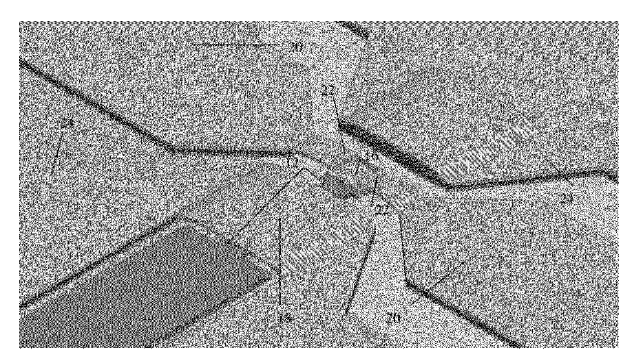
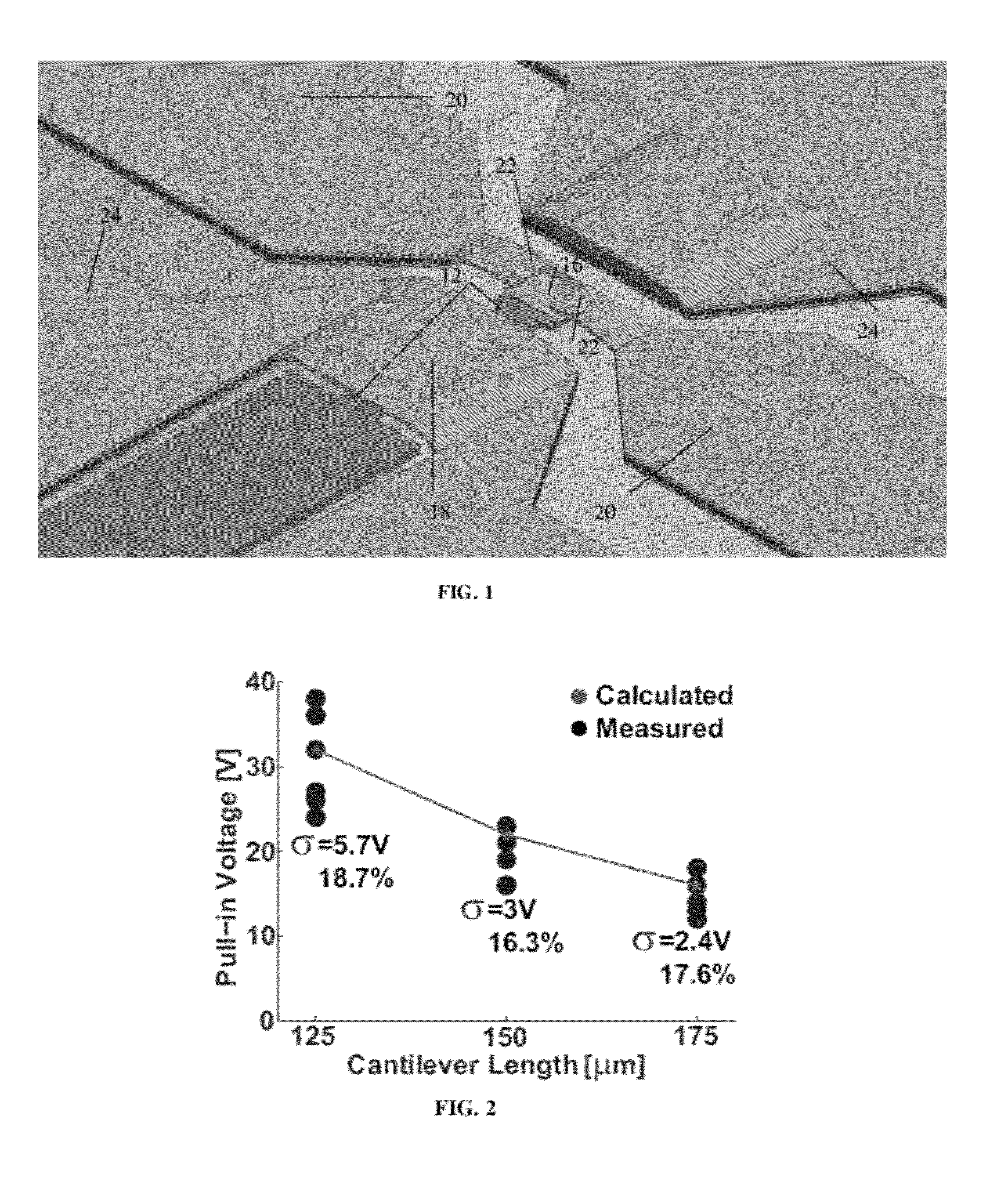
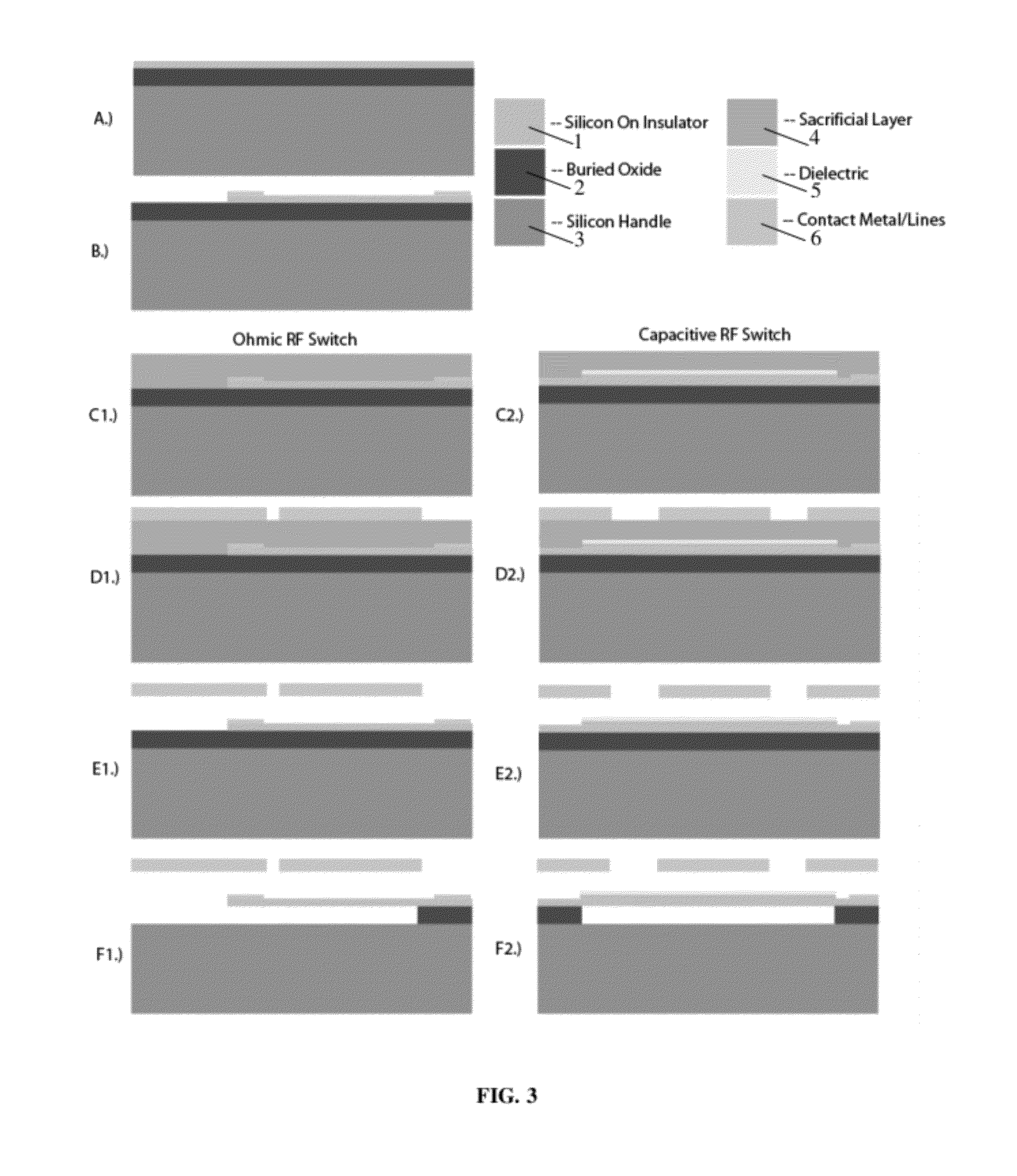
[0037]The present invention provides a new MEMS switch design that is substantially independent of most or all of the aforementioned process variability. This MEMS switch preferably has a moving part made of undoped monocrystalline silicon. Its monocrystalline nature renders this material among the purest available with significant fewer defects than any other material available in the integrated circuit industry...


PUM


Abstract

A radio frequency (RF) micro-electro-mechanical systems (MEMS) switch and high yield manufacturing method. The switch can be fabricated with very high yield despite the high variability of the manufacturing process parameters. The switch is fabricated with monocrystalline material, e.g., silicon, as the moving portion. The switch fabrication process is compatible with CMOS electronics fabricated on Silicon-on-Insulator (SOI) substrates. The switch comprises a movable portion having conductive portion selectively positioned with a bias voltage to conductively bridge a gap in a signal line.

Description

CROSS-REFERENCE TO RELATED APPLICATION[0001]This application is a continuation of application Ser. No. 12 / 808,002, filed Jun. 14, 2010, which is the U.S. National Stage of International Application No. PCT / US08 / 86897, filed Dec. 15, 2008, which claims the benefit of Provisional Patent Application No. 61 / 013,537, filed Dec. 13, 2007, which applications are hereby incorporated by reference along with patent application Ser. No. 11 / 963,071, filed Dec. 21, 2007.BACKGROUND OF THE INVENTION[0002]This invention relates to micro-electromechanical systems (MEMS) and, more particularly, MEMS switches.[0003]Radio frequency MEMS technology has been under development for nearly two decades now. In this technology, integrated circuits are fabricated with miniaturized mechanical moving parts (e.g., beams and plates) that can be actuated in a variety of ways including electrostatically, magnetically, electrothermally, piezoelectrically and others. The induced mechanical movement reconfigures the el...

Claims


Application Information

Patent Timeline
Patent Type & Authority Applications(United States)
IPC IPC(8): H01H59/00
CPCH01H59/0009H01H1/0036
Inventor PEROULIS, DIMITRIOSFRUEHLING, ADAM
Owner PEROULIS DIMITRIOS
Why Eureka
Try Eureka