
Lead line structure and display panel having the same
a technology of lead line and display panel, which is applied in the field of lead line structure and display panel, can solve the problems of differences in resistance of these lead lines, and achieve the effect of narrowing the length of the fan-out structure and reducing signal delay differences
- Summary
- Abstract
- Description
- Claims
- Application Information
AI Technical Summary
Benefits of technology
Problems solved by technology
Method used
Image

Examples
Embodiment Construction
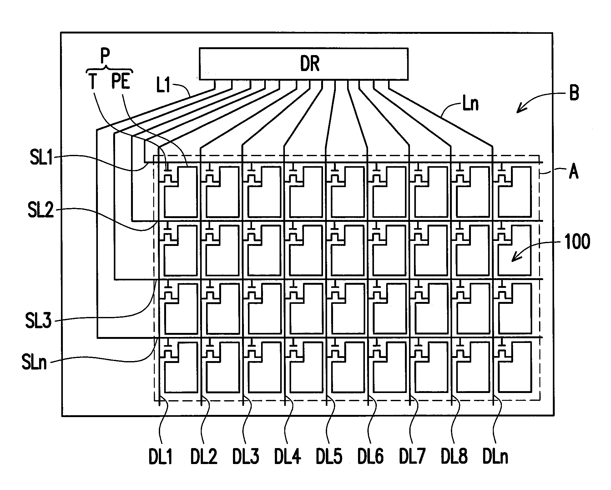
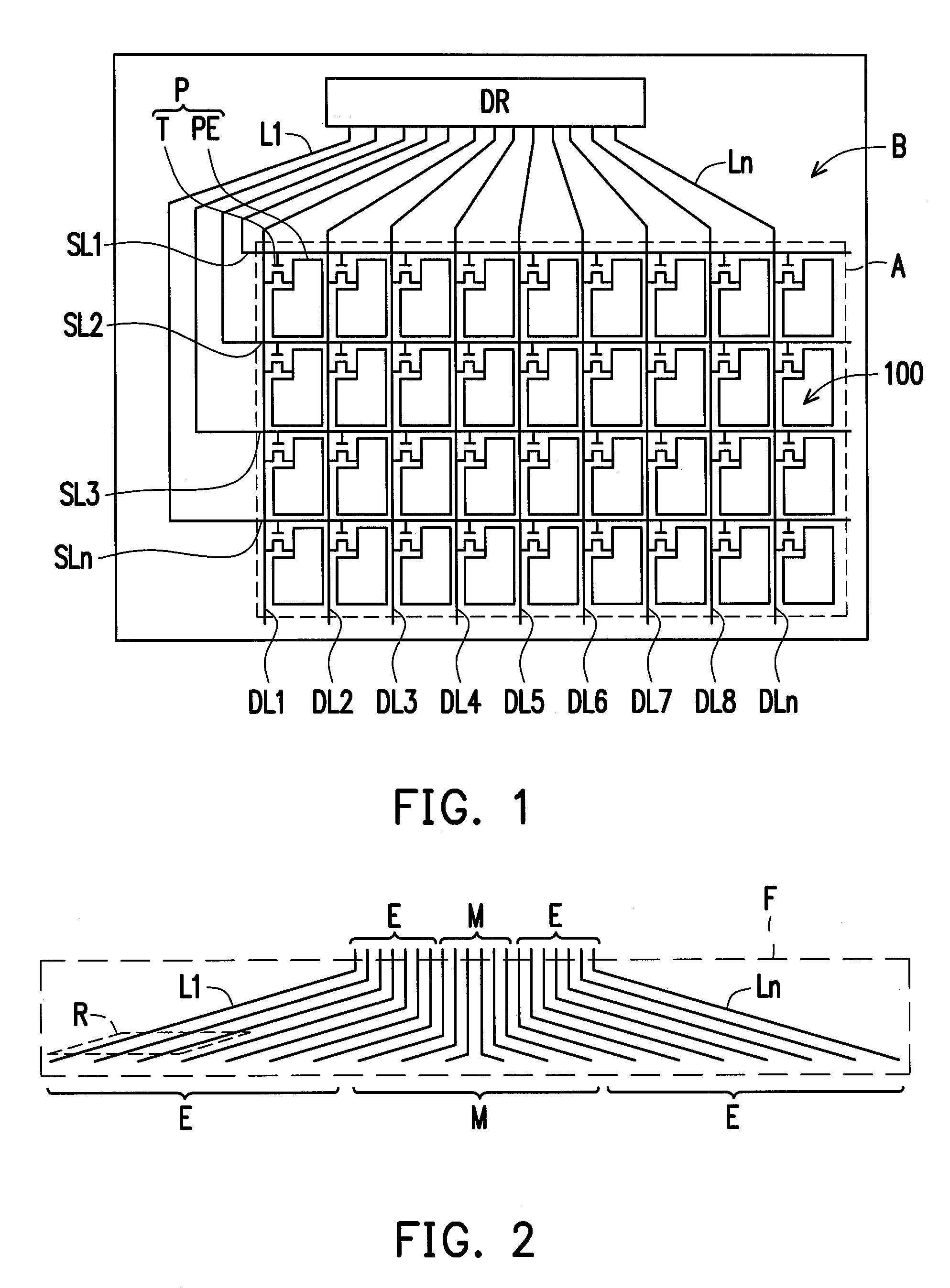
[0022]FIG. 1 is a schematic top view showing a display panel according to an embodiment of the present invention. FIG. 2 is a schematic diagram showing a lead line structure of the display panel of FIG. 1. Referring to FIG. 1 and FIG. 2, a display panel has of the present embodiment has a display region A and a non-display region B and includes a pixel array 100, at least one driving device DR and a plurality of lead lines L1˜Ln.
[0023]The pixel array 100 is disposed on a substrate and disposed in the display region A. In the embodiment, the pixel array 100 comprises a plurality of scan lines SL1˜SLn, a plurality of data lines DL1˜DLn and a plurality of pixel units P.
[0024]The scan lines SL1˜SLn cross over the data lines DL1˜DLn, and an insulation layer is sandwiched between the scan lines SL1˜SLn and the data lines DL1˜DLn. That is to say, extension directions of the data lines DL1˜DLn are not parallel to extension directions of the scan lines SL1˜SLn. Preferably, the extension dire...
PUM
 Abstract
Description
Claims
Application Information