Method for fabrication of iii-nitride device and the iii-nitride device thereof

a technology of nitride and iiinitride, which is applied in the direction of solid-state devices, basic electric elements, electric devices, etc., can solve the problems of device fabricated on si, device with lower resistance rsub>on /sub>, and maximum breakdown voltage (vsub>bd/sub>) limited by the si substrate itself, so as to achieve low leakage and high blocking voltage

Active Publication Date: 2012-12-27
INTERUNIVERSITAIR MICRO ELECTRONICS CENT (IMEC VZW) +1
View PDF1 Cites 29 Cited by
  • Summary
  • Abstract
  • Description
  • Claims
  • Application Information

AI Technical Summary

Benefits of technology

[0007]Such a device can have a lower leakage at elevated voltage compared to the devices without said trench. This is because an additional parallel conduction path along the active-layer-stack / substrate interface, which may for example be an AlN / Si interface, may be substantially eliminated and therefore a device with a relatively high blocking voltage may be achieved.

Problems solved by technology

These devices offer lower on-resistance RON (due to the formation of 2-DEG in un-doped GaN-channel) and high breakdown voltage due to AlGaN buffer.
However, devices fabricated on Si have the disadvantage that the maximum breakdown voltage (VBD) is limited by the Si substrate itself due to its lower critical electrical field strength (0.3 MV / cm) compared to Al(GaN) materials.
This leads to an unwanted leakage path across the AlN / Si inversion interface and therefore VBD is limited by the thickness of the buffer.

Method used


Image

  • Method for fabrication of iii-nitride device and the iii-nitride device thereof
  • Method for fabrication of iii-nitride device and the iii-nitride device thereof
  • Method for fabrication of iii-nitride device and the iii-nitride device thereof

Examples


Embodiment Construction

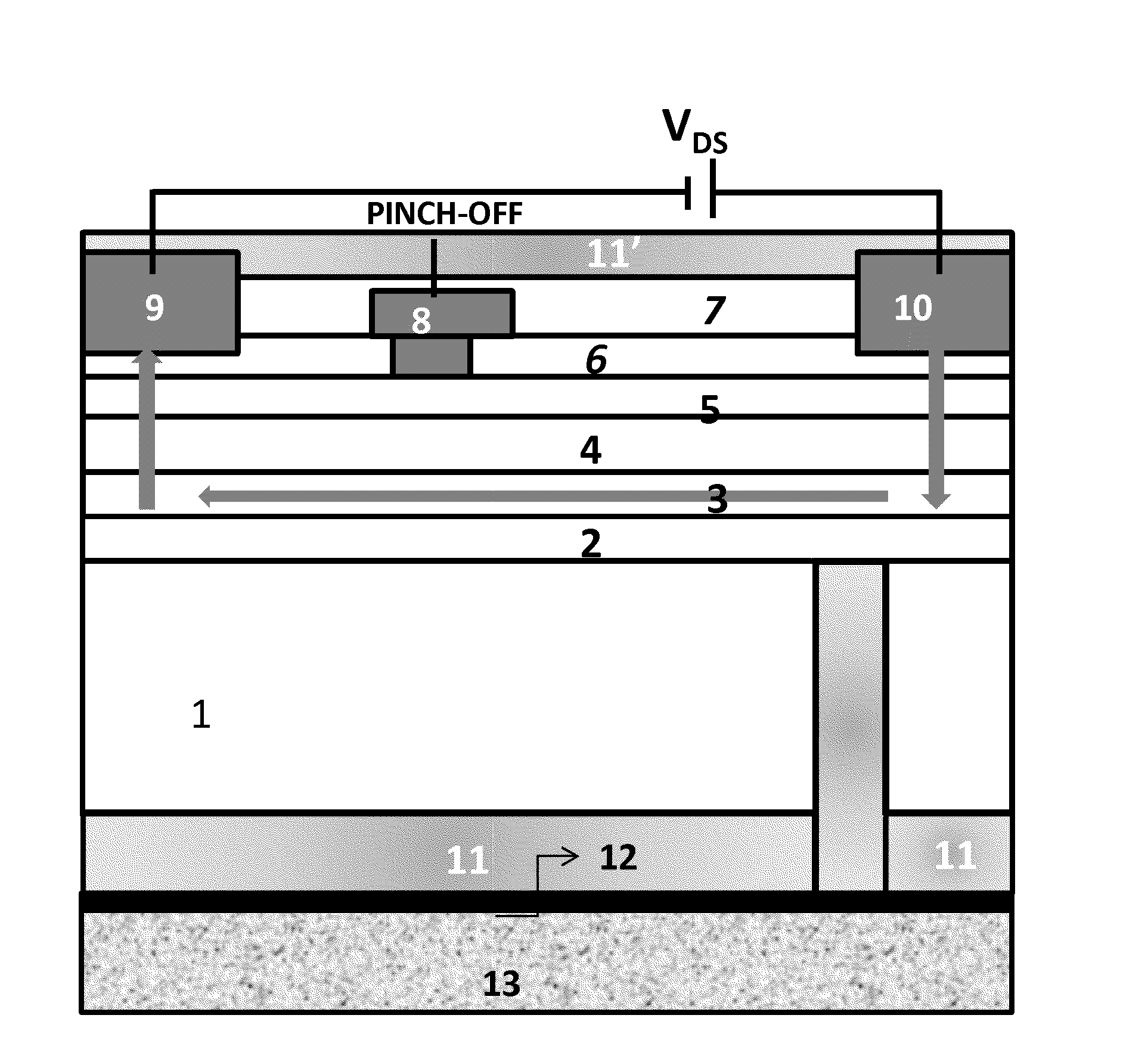
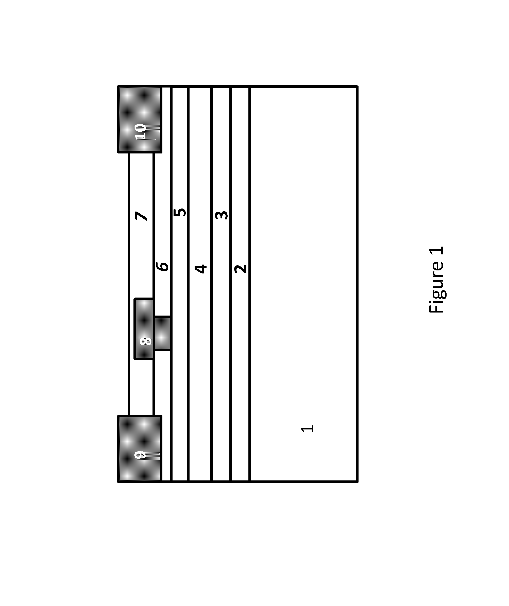
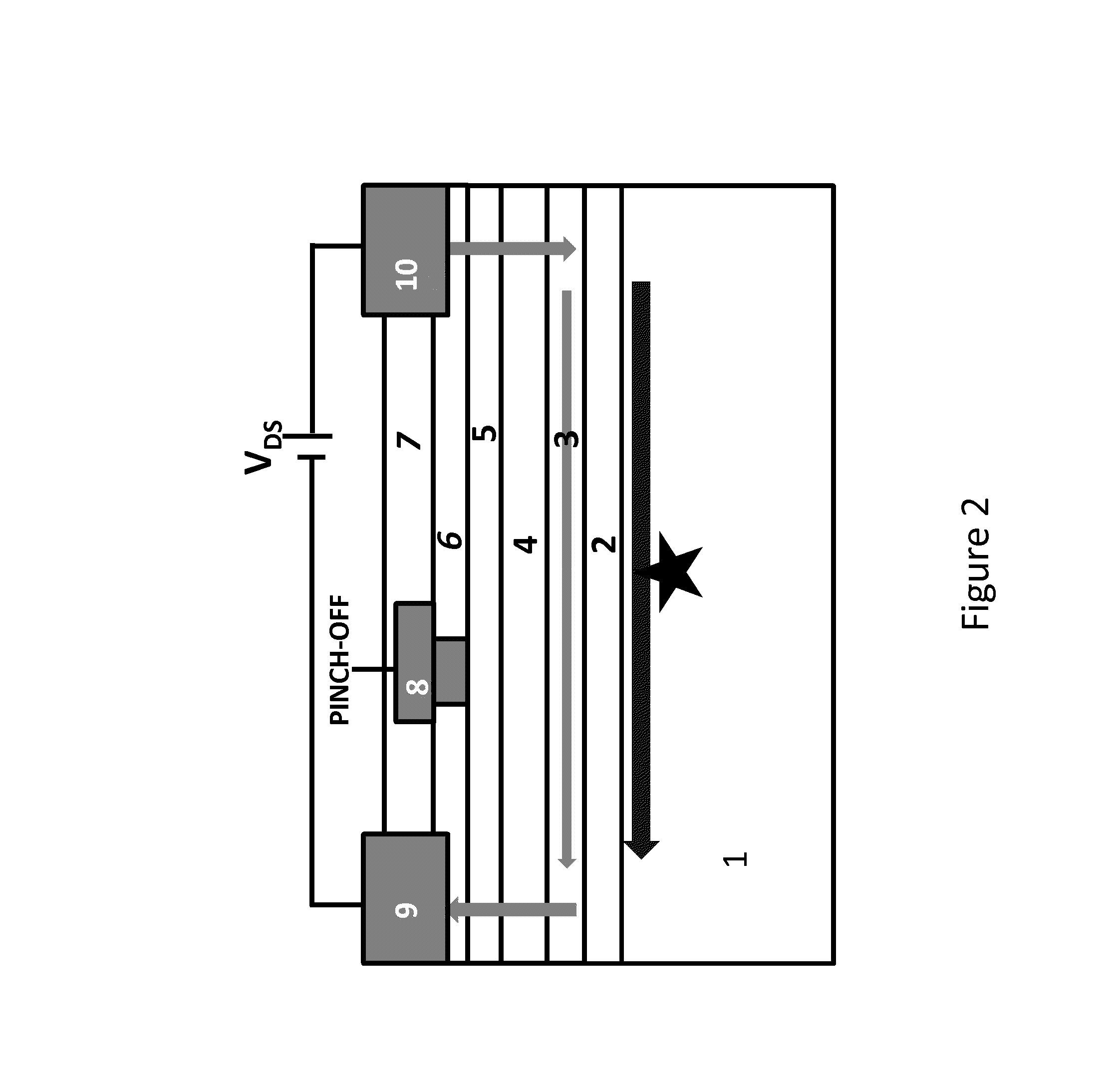
[0035]The present disclosure will be described with respect to particular embodiments and with reference to certain drawings but the disclosure is not limited thereto but only by the claims. The drawings described are only schematic and are non-limiting. In the drawings, the size of some of the elements may be exaggerated and not drawn on scale for illustrative purposes. The dimensions and the relative dimensions do not necessarily correspond to actual reductions to practice of the disclosure.

[0036]Furthermore, the terms first, second, third and the like in the description and in the claims, are used for distinguishing between similar elements and not necessarily for describing a sequential or chronological order. The terms are interchangeable under appropriate circumstances and the embodiments of the disclosure can operate in other sequences than described or illustrated herein.

[0037]Moreover, the terms top, bottom, over, under and the like in the description and the claims are use...


PUM


Abstract

A III-nitride device is provided comprising a semiconductor substrate; a stack of active layers on the substrate, each layer comprising a III-nitride material; a gate, a source and a drain contact on the stack, wherein a gate, a source and a drain region of the substrate are projections of respectively the gate, the source and the drain contact in the substrate; and a trench in the substrate extending from a backside of the substrate (side opposite to the one in contact with the stack of active layers) to an underlayer of the stack of active layers in contact with the substrate, the trench completely surrounding the drain region, being positioned in between an edge of the gate region towards the drain and an edge of the drain region towards the gate and having a width such that the drain region of the substrate is substantially made of the semiconductor material.

Description

CROSS-REFERENCE TO RELATED APPLICATIONS[0001]This application claims the benefit under 35 U.S.C. §119(e) of U.S. provisional application Ser. No. 61 / 499,981 filed on Jun. 22, 2011, the disclosure of which is hereby expressly incorporated by reference in its entirety and is hereby expressly made a portion of this application.FIELD OF THE DISCLOSURE[0002]Semiconductor devices and methods for manufacturing the same are provided. More particularly, a method for manufacturing a III-nitride device and the III-nitride device thereof are provided.BACKGROUND OF THE DISCLOSURE[0003]GaN-based materials have excellent properties for application in power transistors for low loss and high power switching. The AlGaN / GaN / AlGaN double-heterostructure FETs (DHFETs) configuration is extremely promising for high power applications due to the improved carrier confinement.[0004]These devices offer lower on-resistance RON (due to the formation of 2-DEG in un-doped GaN-channel) and high breakdown voltage d...

Claims


Application Information

Patent Timeline
Patent Type & Authority Applications(United States)
IPC IPC(8): H01L29/78H01L21/336
CPCH01L23/36H01L29/0657H01L29/2003H01L29/7783H01L2924/0002H01L2924/00H01L29/0653
Inventor SRIVASTAVA, PUNEETVAN HOVE, MARLEENMALINOWSKI, PAWEL
Owner INTERUNIVERSITAIR MICRO ELECTRONICS CENT (IMEC VZW)
Why Eureka
Try Eureka