Semiconductor device

a technology of semiconductor devices and shielding elements, applied in the direction of semiconductor devices, semiconductor/solid-state device details, electrical equipment, etc., can solve the problem that the shielding element may not work insufficiently

Active Publication Date: 2012-12-27
SEMICON COMPONENTS IND LLC
View PDF8 Cites 32 Cited by
  • Summary
  • Abstract
  • Description
  • Claims
  • Application Information

AI Technical Summary

Problems solved by technology

However, in a case of an ESD protection element using finger form electrodes in which a plurality of finger form source electrodes and a plurality of finger form drain electrodes are inserted therebetwe

Method used


Image

  • Semiconductor device
  • Semiconductor device
  • Semiconductor device

Examples


Embodiment Construction

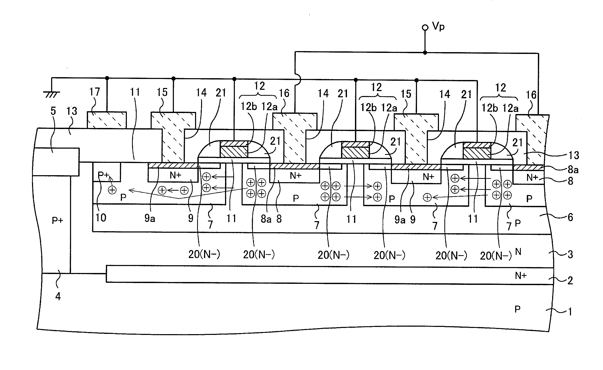
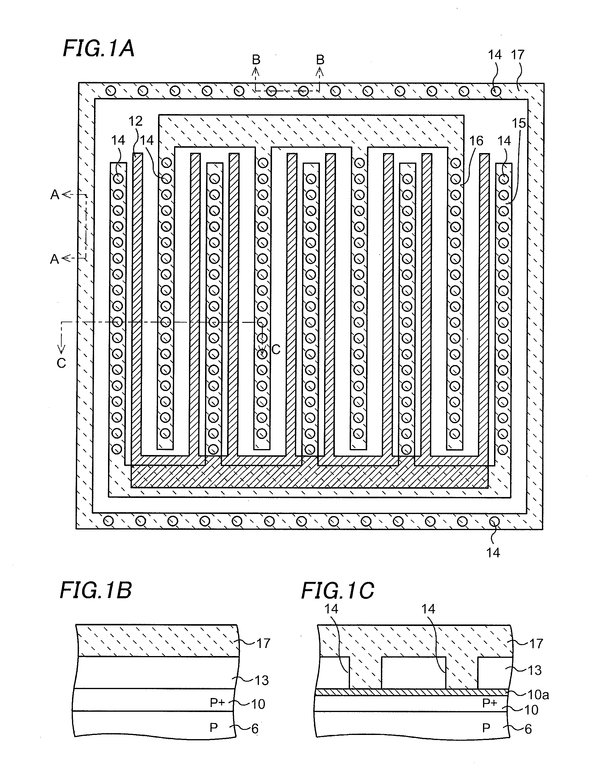
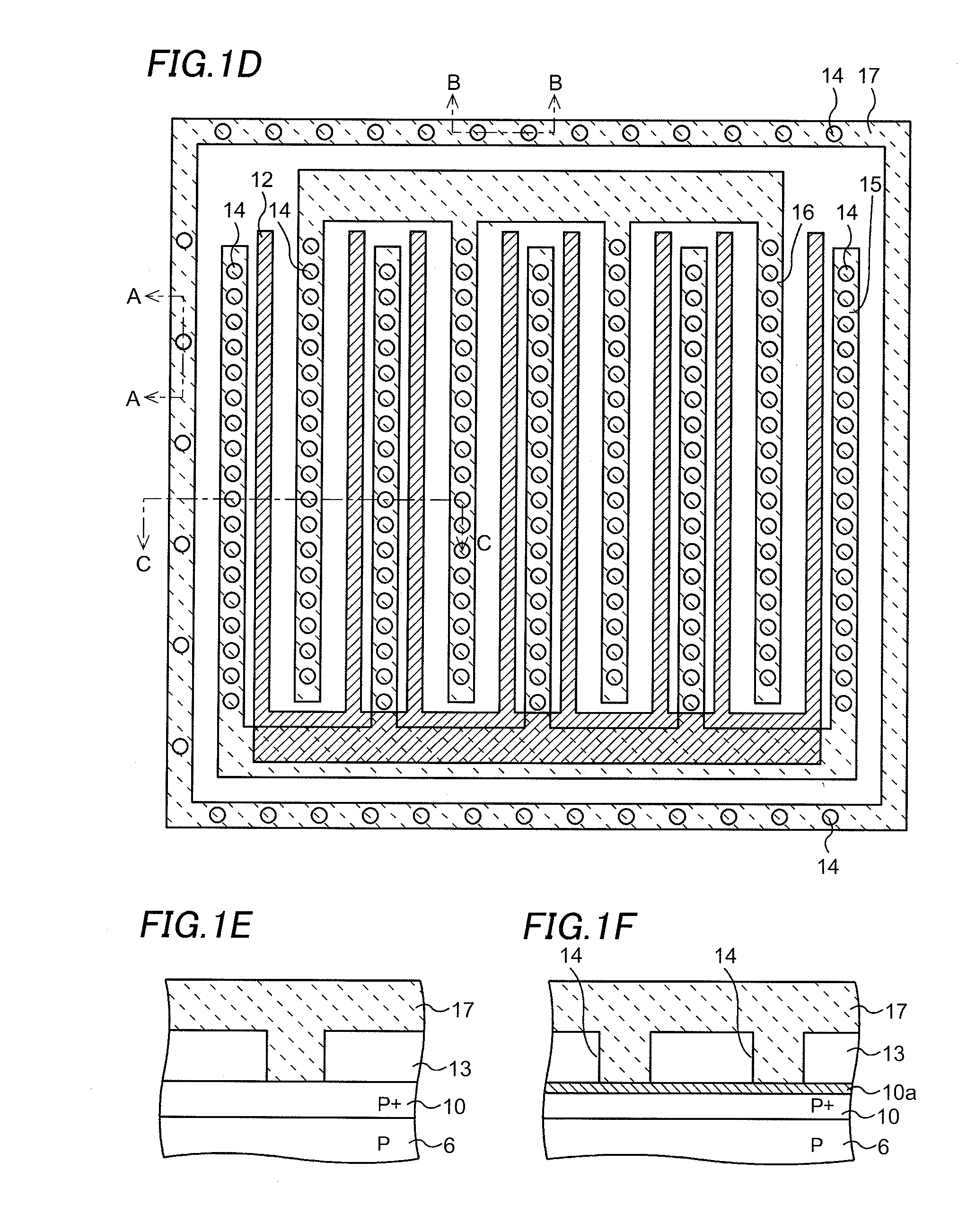
[0029]The feature of a MOS transistor as an ESD protection element of an embodiment will be described hereafter referring to FIGS. 1A to 5. FIG. 1A is a plan view of the ESD protection element of the embodiment, FIG. 1B is a cross-sectional view of FIG. 1A along line A-A, and FIG. 1C is a cross-sectional view of FIG. 1A along line B-B. FIG. 2 is a cross-sectional view of a main portion of FIG. 1A along line C-C.

[0030]Furthermore, FIG. 3A is a plan view of an ESD protection element of a comparative example, FIG. 3B is a cross-sectional view of FIG. 3A along line D-D, and FIG. 3C is a cross-sectional view of FIG. 3A along line E-E. FIG. 4 is a cross-sectional view of a main portion of FIG. 3A along line F-F.

[0031]As shown in FIG. 2, in the MOS transistor as the ESD protection element of the embodiment, an N type epitaxial layer 3 is deposited on a P type semiconductor substrate 1 and an N+ type buried layer 2 is formed in a boundary region of these. The N type epitaxial layer 3 is div...


PUM


Abstract

A semiconductor device equally turns on the parasitic bipolar transistors in the finger portions of the finger form source and drain electrodes when a surge voltage is applied, even with the P+ type contact layer surrounding the N+ type source layers and the N+ type drain layers connected to the finger form source and drain electrodes. A P+ type contact layer surrounds N+ type source layers and N+ type drain layers. Metal silicide layers are formed on the N+ type source layers, the N+ type drain layers, and a portion of the P+ type contact layer. Finger form source electrodes, finger form drain electrodes, and a P+ type contact electrode surrounding these finger form electrodes are formed, being connected to the metal silicide layers respectively through contact holes formed in an interlayer insulation film deposited on the metal silicide layers.

Description

CROSS-REFERENCE OF THE INVENTION[0001]This application claims priority from Japanese Patent Application No. 2011-138448, the content of which is incorporated herein by reference in its entirety.BACKGROUND OF THE INVENTION[0002]1. Field of the Invention[0003]The invention relates to a semiconductor device, in particular, an ESD protection element including a MOS transistor having a high ESD protection characteristic.[0004]2. Description of the Related Art[0005]An LDMOS transistor as well as IGBT has higher switching performance and more stable performance than a bipolar type power transistor, and thus it is widely used in an inverter circuit for a switching power supply such as a DC-DC converter, an inverter circuit for a motor or a lighting device, and so on. The LDMOS is an abbreviation of a Lateral Double Diffused Metal Oxide Semiconductor and means a lateral double-diffused gate MOS. The ESD is an abbreviation of Electro-Static Discharge and means the discharge of static electric...

Claims


Application Information

Patent Timeline
IPC IPC(8): H01L23/60
CPCH01L29/41758H01L29/4238H01L29/4933H01L29/665H01L27/0277H01L27/0207H01L29/0692H01L29/1045H01L29/1087H01L21/823425H01L29/7833
Inventor OTSURU, YUZOTAKEDA, YASUHIROSUGIHARA, SHIGEYUKIINOUE, SHINYA
Owner SEMICON COMPONENTS IND LLC
Why Eureka
Try Eureka