Semiconductor package having electrode on side surface, and semiconductor device

a semiconductor and side surface technology, applied in the field of semiconductor packages, can solve the problems of increasing the size of the semiconductor package, the size of the side external electrode, etc., and achieve the effect of shortening the connection distance between the semiconductor package and suppressing the upsizing of the semiconductor packag

Inactive Publication Date: 2012-12-27
PANASONIC CORP
View PDF3 Cites 15 Cited by
  • Summary
  • Abstract
  • Description
  • Claims
  • Application Information

AI Technical Summary

Benefits of technology

[0009]The present invention solves the above-described conventional problem, and its object is to provide a semiconductor package and a semiconductor device capable of suppressing upsizing of the semiconductor package due to an increase in the number of sidewall external electrodes or side external electrodes formed on side surfaces of the semiconductor package, and shortening a connection distance between the semiconductor packages.

Problems solved by technology

However, in the above-described configuration, since the side external electrodes are formed on the side surfaces of the semiconductor chips, the sizes of the side external electrodes are small.
However, such a configuration increases the number of external connections via the electrodes of the semiconductor package, and hence increases the size of the semiconductor package.

Method used


Image

  • Semiconductor package having electrode on side surface, and semiconductor device
  • Semiconductor package having electrode on side surface, and semiconductor device
  • Semiconductor package having electrode on side surface, and semiconductor device

Examples


embodiment 1

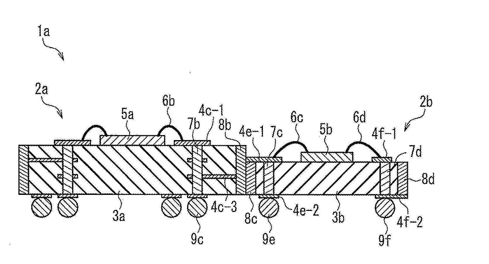
[0057]FIG. 1A is a perspective view showing a configuration of a semiconductor package 2a according to Embodiment 1 of the present invention. FIG. 1B is a cross-sectional view taken along a line A-A in FIG. 1A.

[0058]As shown in FIG. 1B, four layers of electrical passages 4a-1 to 4a-4 are stacked in a substrate 3a. Each of the electrical passages 4a-1 to 4a-4 is formed by patterning. A semiconductor chip 5a is disposed on the substrate 3a. A wire 6a connects the semiconductor chip 5a and the first layer of the electrical passage 4a-1. A via 7a is formed in the substrate 3a. The via 7a passing through the substrate 3a connects each of the electrical passages 4a-1 to 4a-4.

[0059]A side external electrode 8a is formed on a side surface of the substrate 3a. The side external electrode 8a is connected to the second layer of the electrical passage 4a-2. Thereby, a signal output from the semiconductor chip 5a is transmitted to the surface layer of the electrical passage 4a-1 via the wire 6a,...

embodiment 2

[0073]FIG. 4A is a perspective view showing a configuration of a semiconductor package 2c according to Embodiment 2 of the present invention. FIG. 4B is a partial cross-sectional view taken along a line C-C in FIG. 4A.

[0074]A substrate 13 has a configuration in which four layers of electrical passages 14a-1 to 14a-4 are stacked. Each of the electrical passages is formed by patterning. A semiconductor chip 15 is disposed on the substrate 13 so that a terminal surface of the semiconductor chip 15 is connected to the substrate (face down). Vias 17a-1 to 17a-3 are formed in the substrate 13.

[0075]The via 17a-1 connects the first layer of the electrical passage 14a-1 and the second layer of the electrical passage 14a-2. The via 17a-2 connects the second layer of the electrical passage 14a-2 and the third layer of the electrical passage 14a-3. The via 17a-3 connects the third layer of the electrical passage 14a-3 and the fourth layer of the electrical passage 14a-4.

[0076]A side external e...

embodiment 3

[0084]FIG. 6A is a side view showing a configuration of a semiconductor package 2d according to Embodiment 3 of the present invention. The semiconductor package 2d according to the present embodiment is the same as the semiconductor package 2a according to Embodiment 1, except for the configuration in the vicinity of the side external electrode. In the semiconductor package 2d according to the present embodiment, the same constituent elements as those in the semiconductor package 2a according to Embodiment 1 are denoted with the same reference numerals, and the explanation will not be repeated.

[0085]A side external electrode 28 is formed of four layers of electrical passages 24-1 to 24-4, and cut vias 27a-1 to 27c-1, 27a-2 to 27c-2, 27a-3 to 27c-3 having tapered shapes.

[0086]FIG. 6B is a top view showing the process of forming the side external electrode. A line E-E in FIG. 6B indicates a position to be cut in the later process. FIG. 6C is a perspective view showing a region R in FI...


PUM


Abstract

A semiconductor package includes a substrate, a semiconductor chip disposed on the substrate, and a connection wiring connected electrically to the semiconductor chip. The semiconductor package further includes a sidewall formed of an insulator, an inner electrode formed on a first surface of the sidewall that faces the substrate, and a sidewall external electrode formed on a second surface of the sidewall different from the first surface. The inner electrode and the sidewall external electrode are connected electrically, and the inner electrode is connected to the connection wiring. With this configuration, it is possible to suppress the semiconductor package from being large due to an increase in the number of sidewall external electrodes formed on the side surfaces of the semiconductor package, and to shorten a connection distance between the semiconductor packages by connecting the sidewall external electrodes.

Description

FIELD OF THE INVENTION[0001]The present invention relates to a semiconductor package in which a semiconductor chip is mounted on a substrate, and a semiconductor device configured by combining the semiconductor packages.BACKGROUND OF THE INVENTION[0002]As a configuration example of a semiconductor chip, for example, JP 2008-130932 A discloses a semiconductor chip having an electrode on its side surface.[0003]FIG. 16 is a cross-sectional view showing a configuration of a conventional semiconductor chip 101 having a side external electrode. The semiconductor chip 101 includes a circuit region 103 formed on a substrate 102, and an electrode pad 104 connected to the circuit region 103. The electrode pad 104 is formed so as to extend to side surfaces of the substrate 102, and functions as a side external electrode.[0004]Such a side external electrode is formed in the following manner. A plurality of circuit regions are formed on a wafer, and conductive portions serving as electrode pads ...

Claims


Application Information

Patent Timeline
Patent Type & Authority Applications(United States)
IPC IPC(8): H01L23/48
CPCH01L23/49805H01L23/49827H01L25/105H01L24/48H01L2224/16225H01L2224/48227H01L2924/15311H01L2924/16195H01L23/057H01L2224/16227H01L2924/12042H01L2224/48091H01L2224/49171H01L2924/00014H01L24/49H01L2924/00H01L2224/45099H01L2224/45015H01L2924/207
Inventor KOBAYASHI, SHOUICHITANAKA, HIROYUKI
Owner PANASONIC CORP
Why Eureka
Try Eureka