Pixel structure and method of driving the same

a technology of pixel structure and method, applied in the field of pixel structure and a method of driving the same, can solve the problems of user denunciation of color washout phenomenon, and achieve the effect of reducing the color washout phenomenon of the display device and improving the aperture ratio of the pixel structur

Inactive Publication Date: 2013-01-03
AU OPTRONICS CORP
View PDF31 Cites 83 Cited by
  • Summary
  • Abstract
  • Description
  • Claims
  • Application Information

AI Technical Summary

Benefits of technology

[0013]In light of the foregoing, the first pixel electrode and the second pixel electrode are disposed in different film layers and are separated from each other by the insulating layer. Therefore, a spacing region for separating the main pixel electrode and the sub-pixel electrode is not required in the pixel structure of the present invention, and the aperture ratio of the pixel structure can be improved. In addition, in an embodiment of the present invention, the first pixel electrode and the second pixel electrode have different voltages though disposing the sharing switch device in the pixel structure, so as to reduce the color washout phenomenon of the display device.

Problems solved by technology

Although the LCD adopting the above-mentioned technologies can achieve the purpose of the wide viewing angle, but the color washout phenomenon is denounced by users.

Method used


Image

  • Pixel structure and method of driving the same
  • Pixel structure and method of driving the same
  • Pixel structure and method of driving the same

Examples


Embodiment Construction

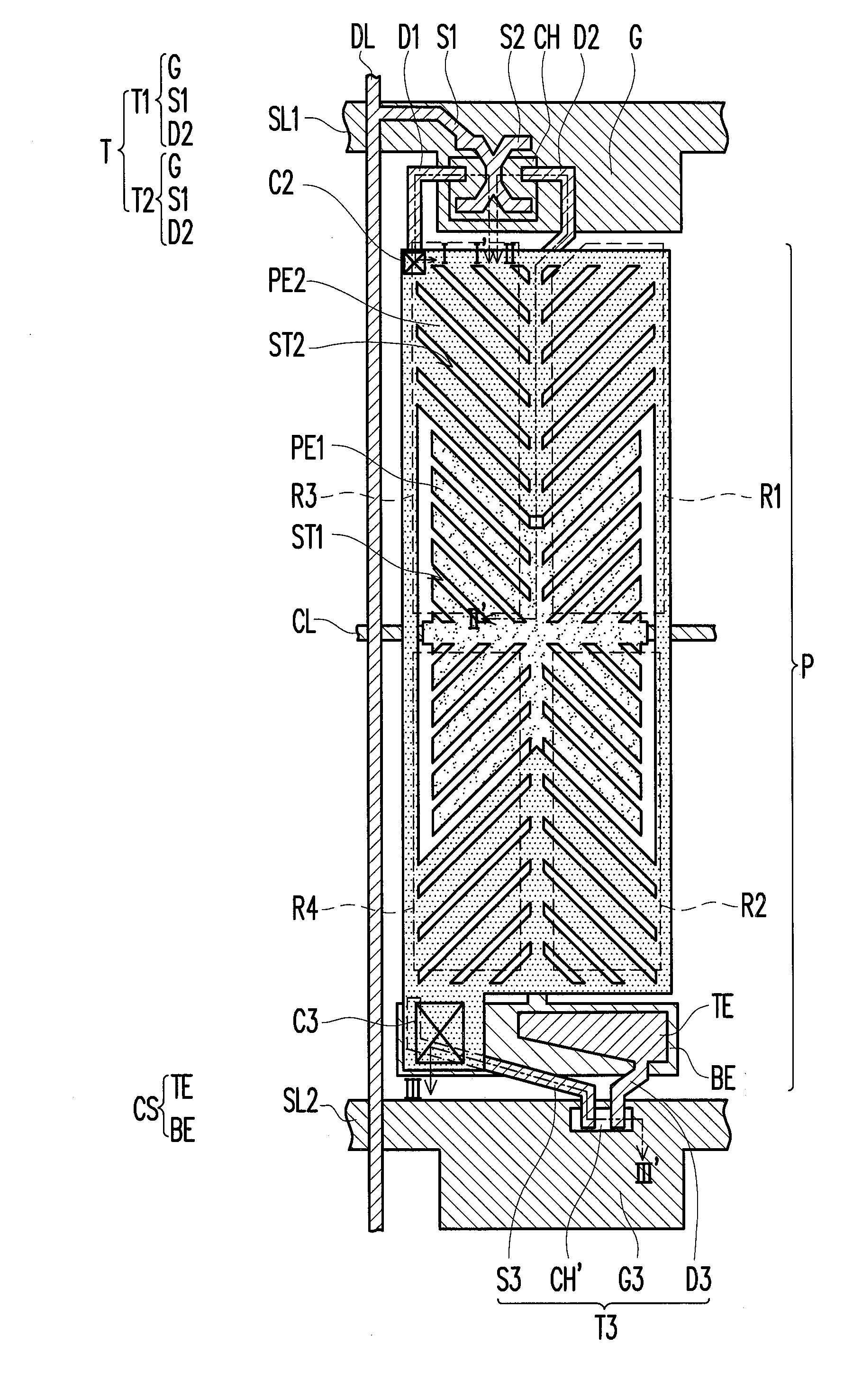
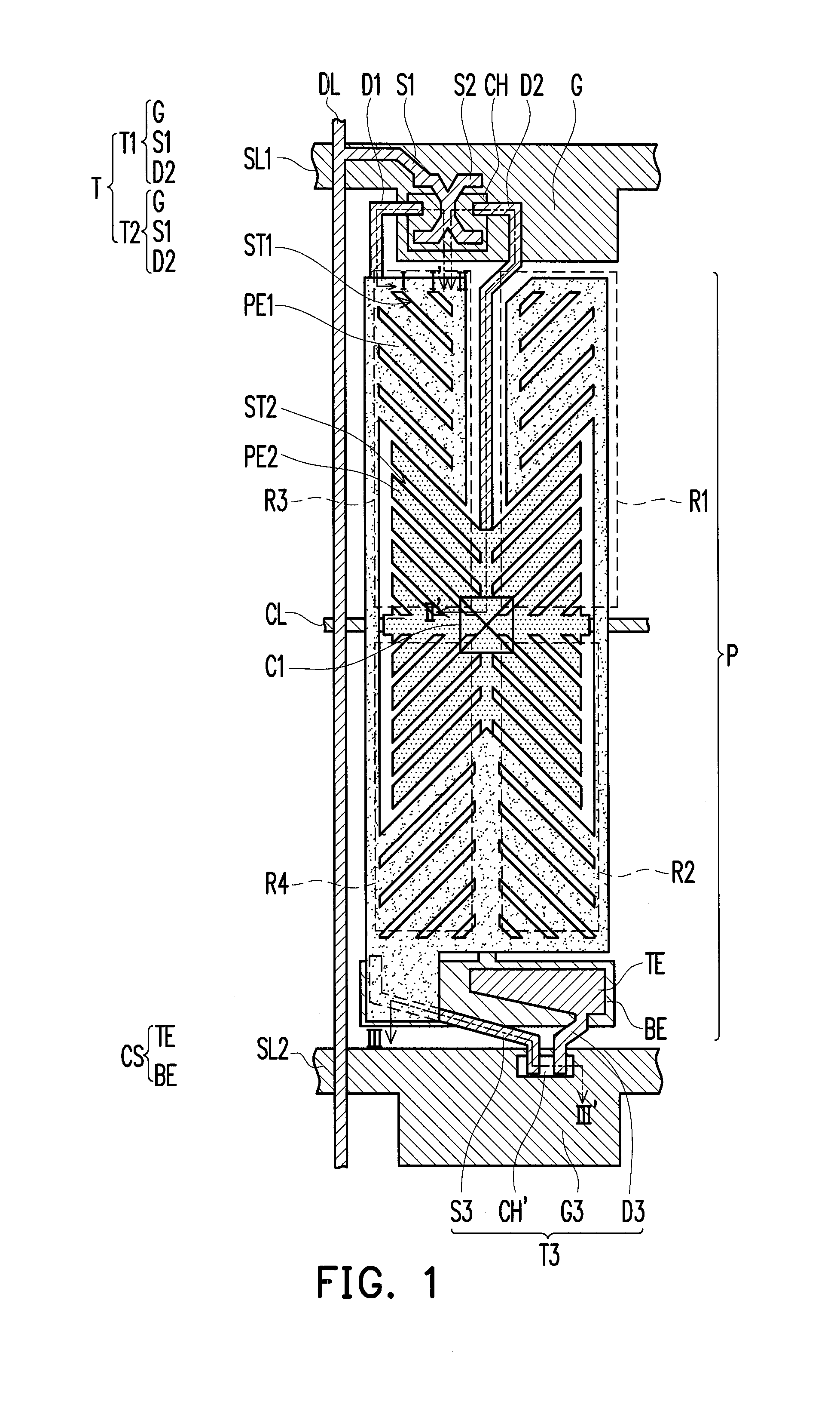
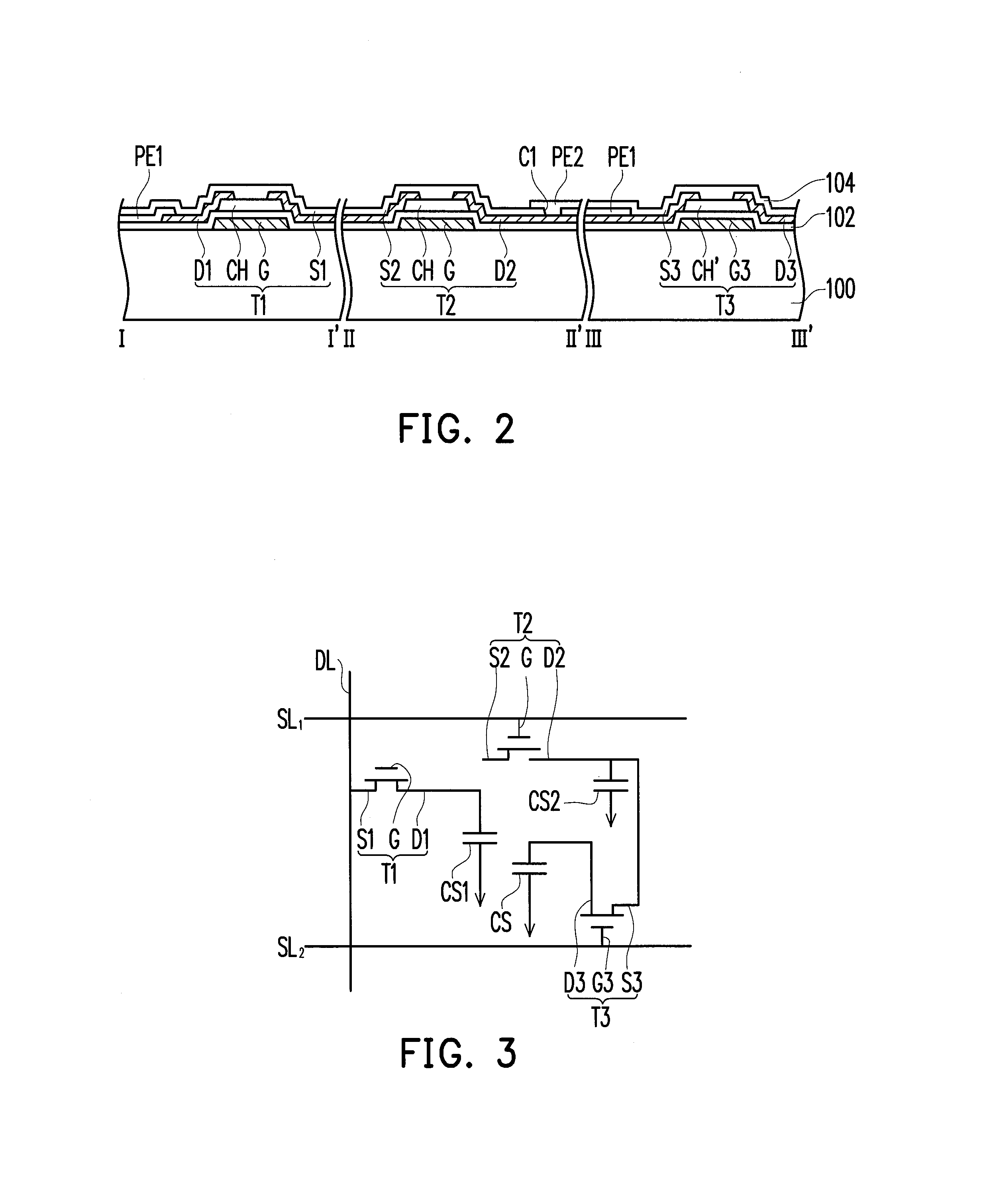
[0025]FIG. 1 is a schematic diagram showing a top view of a pixel structure according to an embodiment of the present invention. FIG. 2 is cross-sectional diagram along the cross-sectional line I-I′, the cross-sectional line II-II′ and the cross-sectional line in FIG. 1. FIG. 3 is a schematic circuit diagram of the pixel structure in FIG. 1. Referring to FIG. 1, FIG. 2 and FIG. 3, the pixel structure is disposed on a substrate 100 and comprises a first scan line SL1, a second scan line SL2, a data line DL, a driving device T, a first pixel electrode PE1, an insulating layer 104, a second pixel electrode PE2 and a sharing switch device T3.

[0026]The substrate 100 can be made of glass, quartz, an organic polymer, an opaque / reflective material (such as a conductive material, metal, wafer, ceramics, or any other appropriate material), or any other appropriate material.

[0027]The first scan line SL1, the second scan line SL2 and the data line DL are located on the substrate 100. In this em...


PUM


Abstract

A pixel structure includes a scan line, a data line, a driving device, a first pixel electrode, an insulating layer and a second pixel electrode. The driving device is electrically connected to the scan line and the data line. The first pixel electrode is electrically connected to the driving device. The insulating layer covers the first pixel electrode. The second pixel electrode is disposed on the insulating layer. The second pixel electrode is electrically connected to the driving device and is not directly connected to or not contacted with the first pixel electrode.

Description

CROSS-REFERENCE TO RELATED APPLICATION[0001]This application claims the priority benefit of Taiwan application serial no. 100122906, filed on Jun. 29, 2011. The entirety of the above-mentioned patent application is hereby incorporated by reference herein and made a part of this specification.BACKGROUND OF THE INVENTION[0002]1. Field of the Invention[0003]The present invention relates to a pixel structure and a method of driving the same, and more particularly, the present invention relates to a pixel structure and a method of driving the same capable of reduce color washout of a display device.[0004]2. Description of Related Art[0005]At present, some of the basic demands on the LCD include properties such as a high contrast ratio, rapid response and wide viewing angle. The technologies capable of providing a wide viewing angle include, for example, multi-domain vertical alignment (MVA), multi-domain horizontal alignment (MHA), twisted nematic plus wide viewing film (TN+film) and in-...

Claims


Application Information

Patent Timeline
Patent Type & Authority Applications(United States)
IPC IPC(8): G06F3/038G09G3/36
CPCG02F1/133345G02F1/134309G02F2201/40G02F2001/134345G02F1/13624G02F1/134345
Inventor LIAO, PEI-CHUNHSU, WEN-HAOWANG, HUI-JUN
Owner AU OPTRONICS CORP
Why Eureka
Try Eureka