Nitride semiconductor light emitting device

Inactive Publication Date: 2013-01-10
SAMSUNG ELECTRONICS CO LTD
View PDF2 Cites 2 Cited by
  • Summary
  • Abstract
  • Description
  • Claims
  • Application Information

AI Technical Summary

Benefits of technology

[0008]An aspect of the present invention provides a nitride semiconductor light emitting device capable of provid

Problems solved by technology

Such a doped high impurity concentration may cause deterioration of crystal pr

Method used


Image

  • Nitride semiconductor light emitting device
  • Nitride semiconductor light emitting device
  • Nitride semiconductor light emitting device

Examples


embodiment

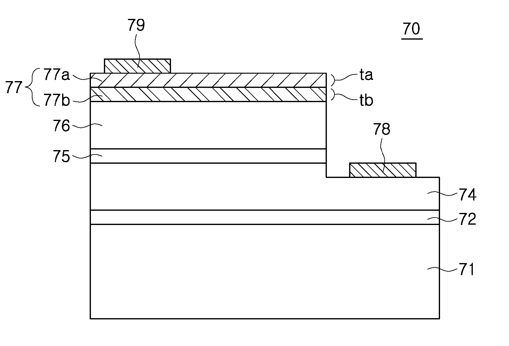
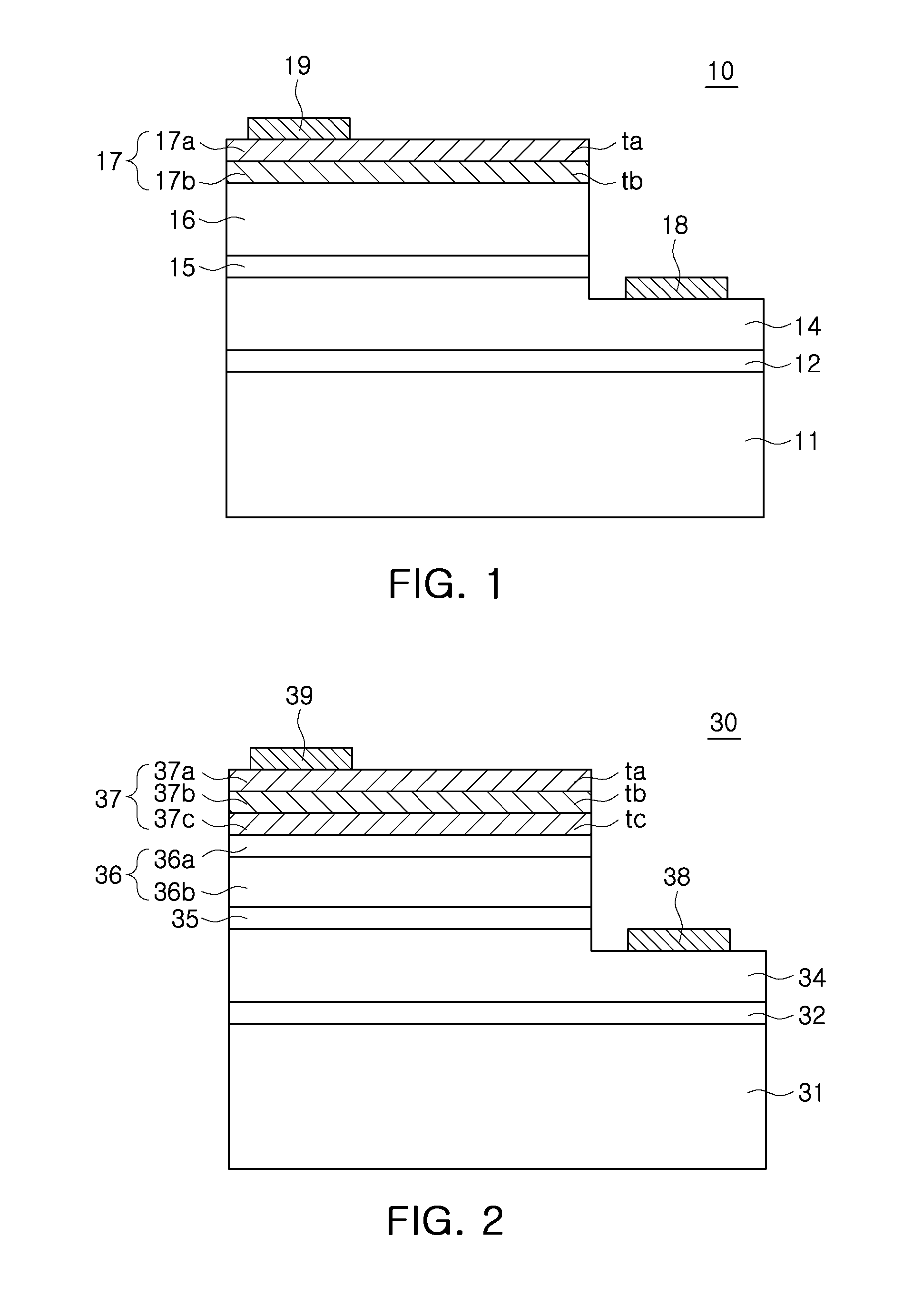
[0050]A first n-type GaN layer having an impurity concentration of 3×10¹⁹ / cm3 and a second n-type GaN layer having an impurity concentration of 5×10²⁰ / cm3 were formed on a sapphire substrate by using metal organic chemical vapor deposition (MOCVD) equipment, and an active layer including six pairs of In0.2Ga0.8N quantum well layers and GaN quantum barrier layers was formed thereon. Subsequently, a p-type Al0.2Ga0.8N electron blocking layer (EBL), which is a p-type nitride layer, and a p-type GaN layer having an impurity concentration of 1×10²⁰ / cm3 were formed thereon.

[0051]Thereafter, a contact layer was formed such that a low concentration second p-type nitride layer was positioned between two high concentration first p-type nitride layers according to an embodiment of the present invention, in particular, a structure shown in FIG. 2. The first p-type nitride layer was formed to have a thickness of about 20 nm and an impurity concentration of 5×10²⁰ / cm3, and the second p-type nitri...


PUM


Abstract

Provided is a nitride semiconductor light emitting device including p-type nitride semiconductor layer, an n-type nitride semiconductor layer, and an active layer formed therebetween. A contact layer is positioned between the p-type nitride semiconductor layer and a p-side electrode. The contact layer includes a first p-type nitride layer having a first impurity concentration to form ohmic contact with the p-side electrode and a second p-type nitride layer having a second impurity concentration, the second impurity concentration having a concentration lower than the first impurity concentration.

Description

CROSS-REFERENCE TO RELATED APPLICATIONS[0001]This application claims the priority of Korean Patent Application No. 10-2011-0066925 filed on Jul. 6, 2011, in the Korean Intellectual Property Office, the disclosure of which is incorporated herein by reference.BACKGROUND OF THE INVENTION[0002]1. Field of the Invention[0003]The present invention relates to a nitride semiconductor light emitting device, and more particularly, to a nitride semiconductor light emitting device having improved light emission efficiency and electrical reliability.[0004]2. Description of the Related Art[0005]Recently, increasing interest has been shown in a nitride semiconductor light emitting device as a light source capable of covering a wide range of wavelengths, including wavelengths in the blue and green light bands, according to a composition rate thereof and a nitride semiconductor light emitting device has been widely used for a full color display, an image scanner, various signal systems and optical c...

Claims


Application Information

Patent Timeline
IPC IPC(8): H01L33/30
CPCH01L33/025H01L29/452H01L33/40H01L33/32H01L33/36
Inventor SHIM, HYUN WOOKLEE, DONG JUSHIN, DONG IKKIM, YOUNG SUNASAI, MAKOTOSOHN, YU RI
Owner SAMSUNG ELECTRONICS CO LTD
Why Eureka
Try Eureka