

Semiconductor device and method for manufacturing semiconductor device
a semiconductor and semiconductor technology, applied in the direction of semiconductor devices, basic electric elements, electrical appliances, etc., can solve the problems of difficult control of circuits and unsuitable drain current flows, and achieve the effects of improving on-state characteristics, high-speed response, and high performan
- Summary
- Abstract
- Description
- Claims
- Application Information
AI Technical Summary
Benefits of technology
Problems solved by technology
Method used
Image

Examples
embodiment 1
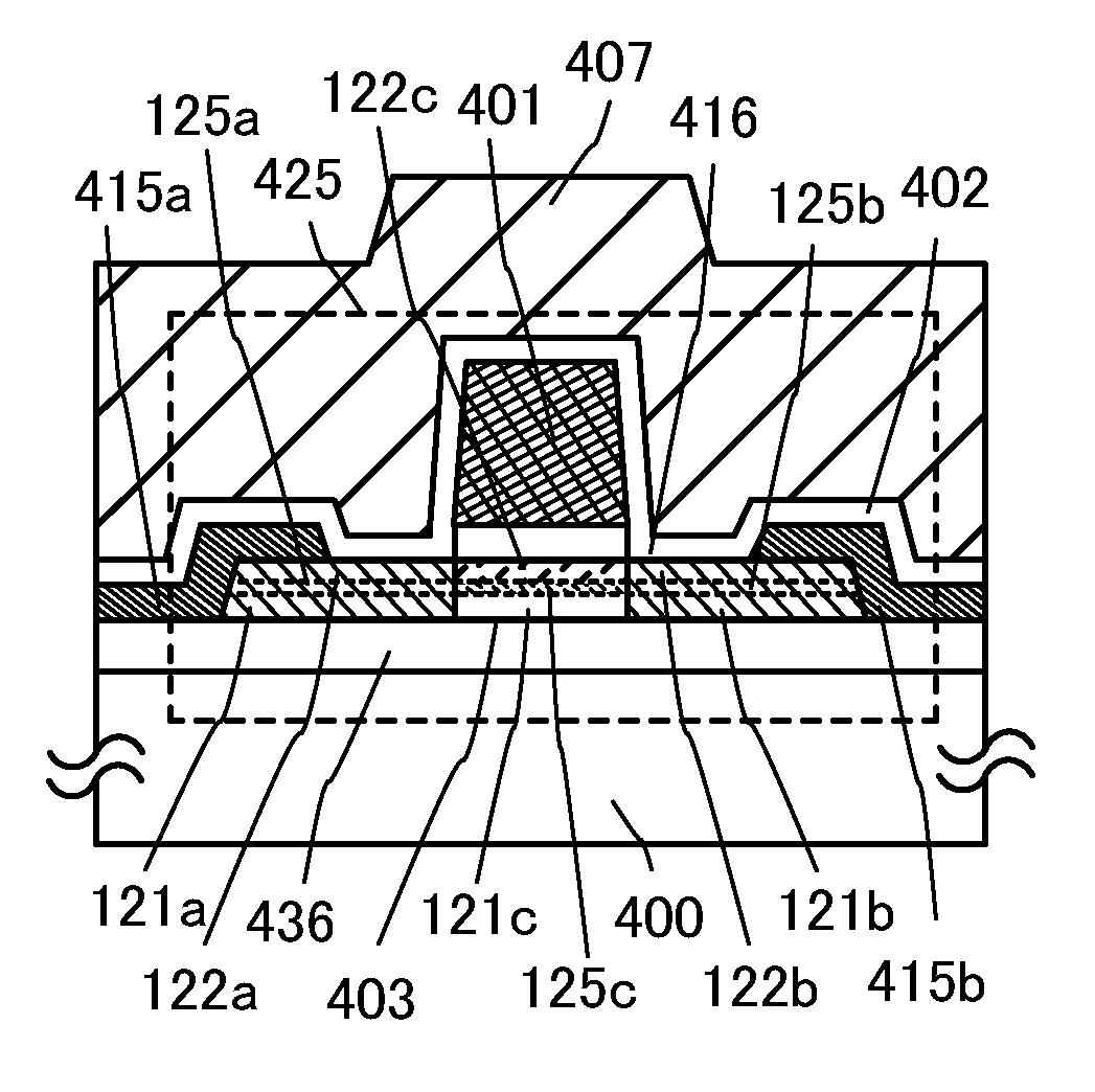
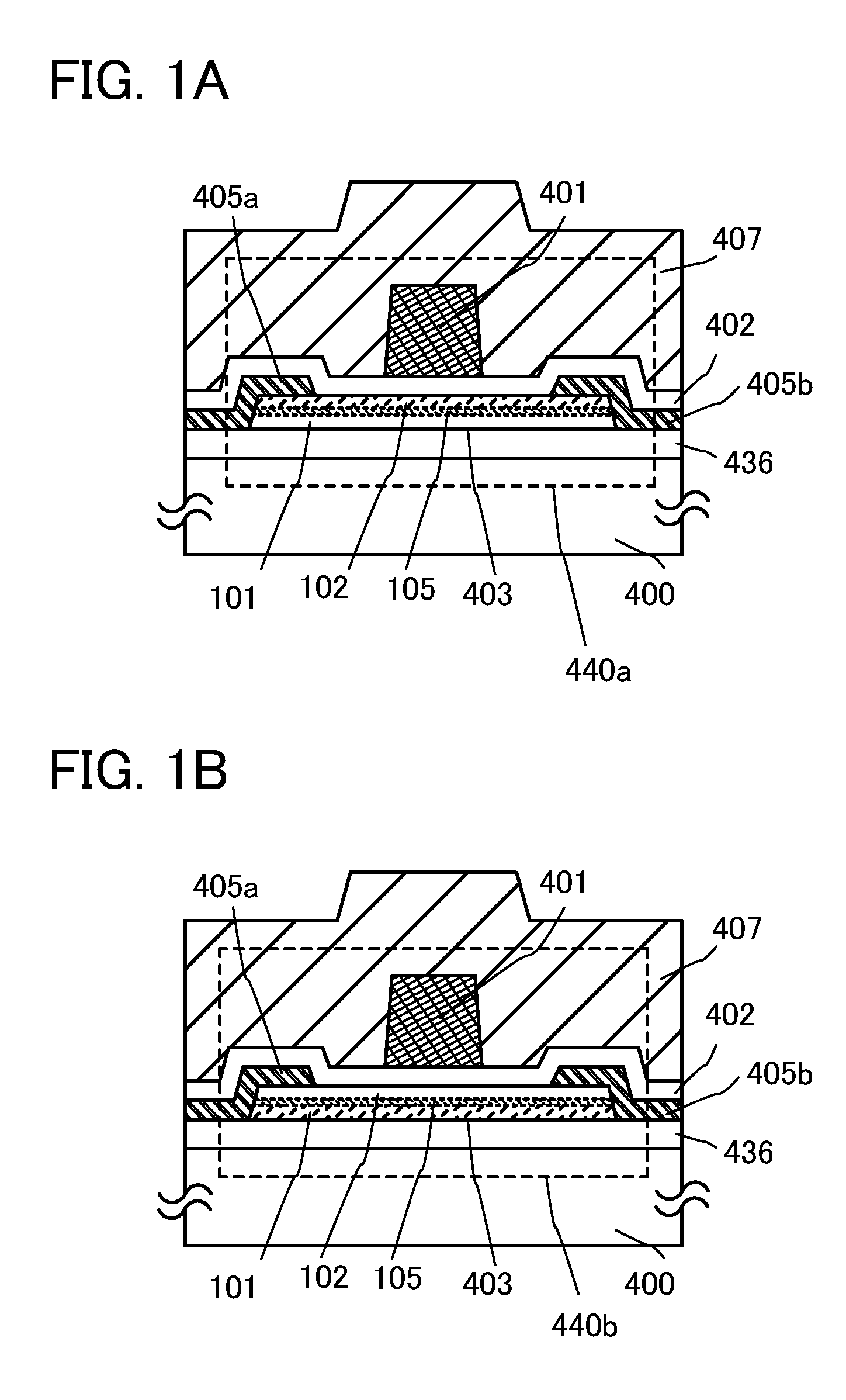
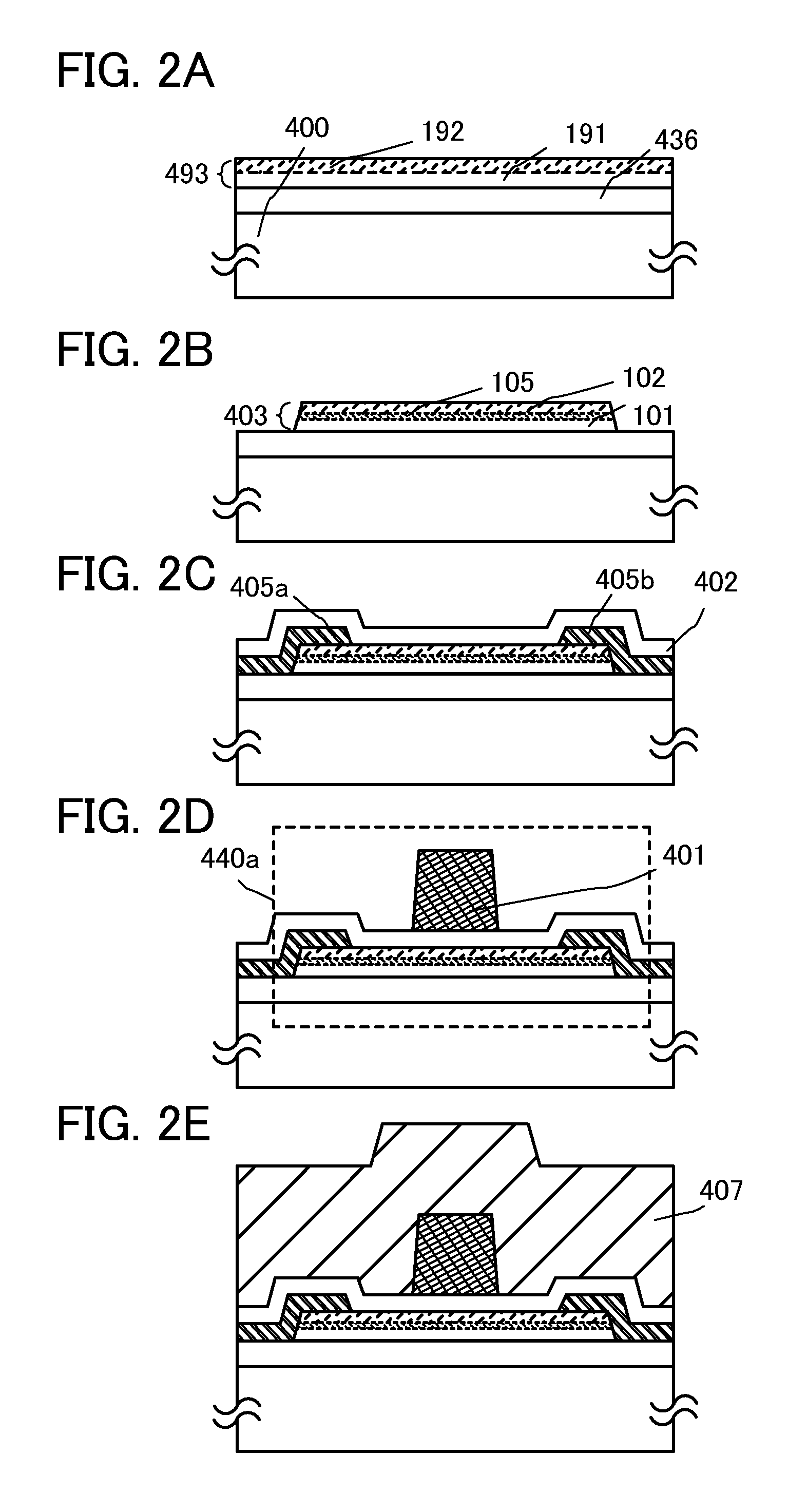
[0068]In this embodiment, one embodiment of a semiconductor device and a method for manufacturing the semiconductor device will be described with reference to FIGS. 1A and 1B, FIGS. 2A and 2E, and FIGS. 3A to 3D. In this embodiment, a transistor including an oxide semiconductor film will be described as an example of the semiconductor device.
[0069]The transistor may have a single-gate structure in which one channel formation region is formed, a double-gate structure in which two channel formation regions are formed, or a triple-gate structure in which three channel formation regions are formed. Alternatively, the transistor may have a dual-gate structure including two gate electrode layers positioned over and under a channel formation region with a gate insulating film provided therebetween.
[0070]A transistor 440a in FIG. 1A and a transistor 440b in FIG. 1B are examples of planar type transistors having a top-gate structure.
[0071]As illustrated in FIGS. 1A and 1B, the transistor 440...
embodiment 2
[0188]In this embodiment, another embodiment of a semiconductor device and a method for manufacturing the semiconductor device will be described with reference to FIGS. 7A to 7C, FIGS. 8A to 8C, and FIGS. 11A and 11B. The same portion as or a portion having a function similar to those in the above embodiment can be formed in a manner similar to that described in the above embodiment, and also the steps similar to those in the above embodiment can be performed in a manner similar to that described in the above embodiment, and repetitive description is omitted. In addition, detailed description of the same portions is not repeated.
[0189]In this embodiment, an example of a structure in which an upper oxide semiconductor layer covers side surfaces of a lower oxide semiconductor layer in an oxide semiconductor stack is shown. Since the side surfaces of the lower oxide semiconductor layer are covered with the upper oxide semiconductor layer, the lower oxide semiconductor layer is in conta...
embodiment 3
[0209]In this embodiment, another embodiment of a semiconductor device and a method for manufacturing the semiconductor device will be described with reference to FIGS. 5A to 5C. The same portion as or a portion having a function similar to those in the above embodiment can be formed in a manner similar to that described in the above embodiment, and also the steps similar to those in the above embodiment can be performed in a manner similar to that described in the above embodiment, and repetitive description is omitted. In addition, detailed description of the same portions is not repeated.
[0210]This embodiment shows, in a method for manufacturing a semiconductor device according to one embodiment of the disclosed invention, oxygen (which includes at least one of an oxygen radical, an oxygen atom, and an oxygen ion) is added to an oxide semiconductor stack which has been subjected to dehydration or dehydrogenation treatment to supply oxygen to the oxide semiconductor film.
[0211]The...
PUM
 Abstract
Description
Claims
Application Information