Semiconductor package and method of manufacturing the same

a technology of semiconductors and semiconductors, applied in the field of semiconductor packages, can solve the problems of complex manufacturing process and increase loss, and achieve the effect of minimizing the electrical connection distance and easy manufacturing

Inactive Publication Date: 2013-01-10
SAMSUNG ELECTRO MECHANICS CO LTD
View PDF7 Cites 119 Cited by
  • Summary
  • Abstract
  • Description
  • Claims
  • Application Information

AI Technical Summary

Benefits of technology

[0012]An aspect of the present invention provides a semiconductor package capable of being easily manufactured while minimizing an electrical connection distance between an antenna and a semiconductor chip.

Problems solved by technology

That is, when a distance between the antenna and the semiconductor chip increases, loss increases.
Therefore, a manufacturing process is complicated.

Method used


Image

  • Semiconductor package and method of manufacturing the same
  • Semiconductor package and method of manufacturing the same
  • Semiconductor package and method of manufacturing the same

Examples


Embodiment Construction

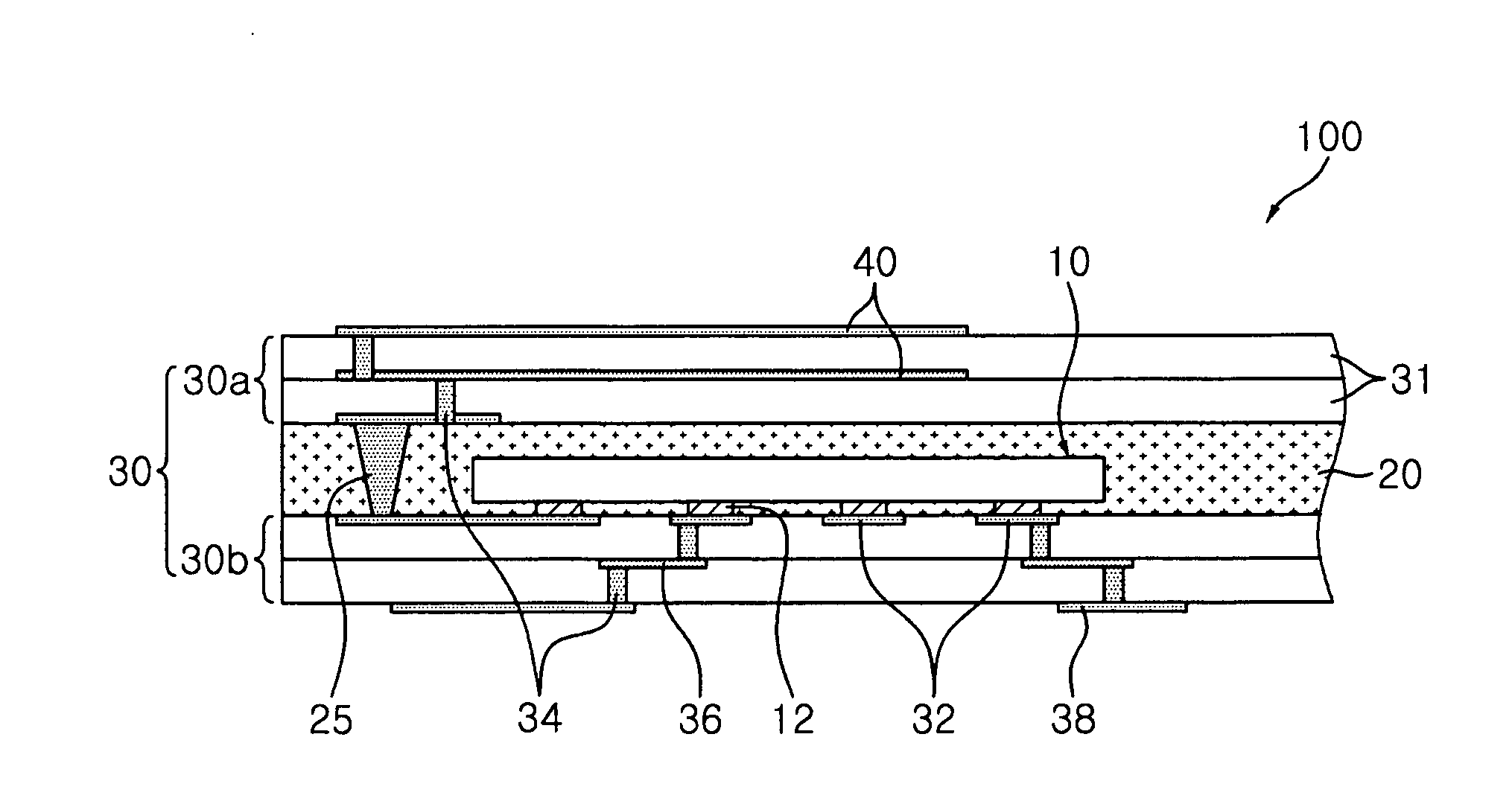
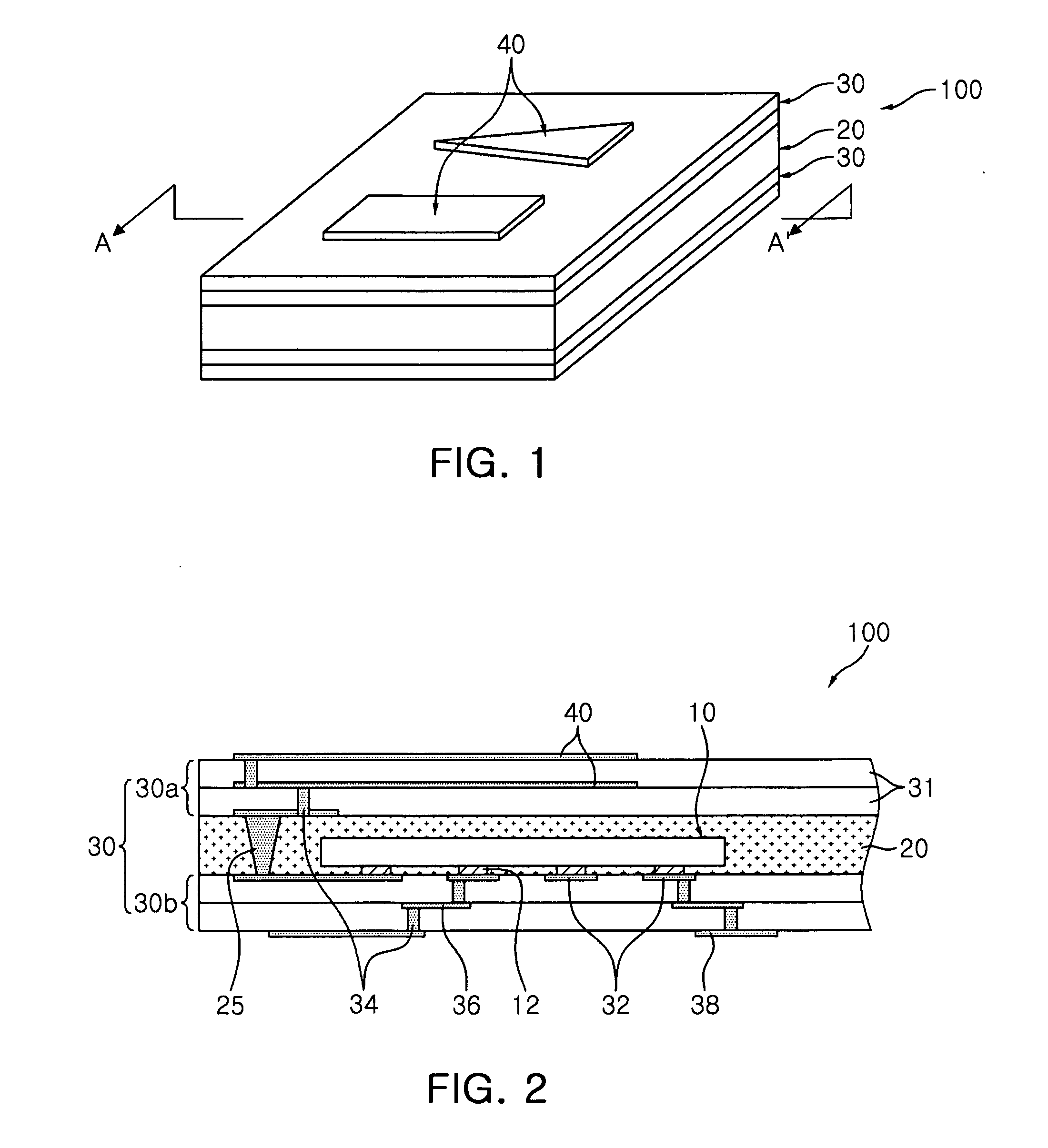
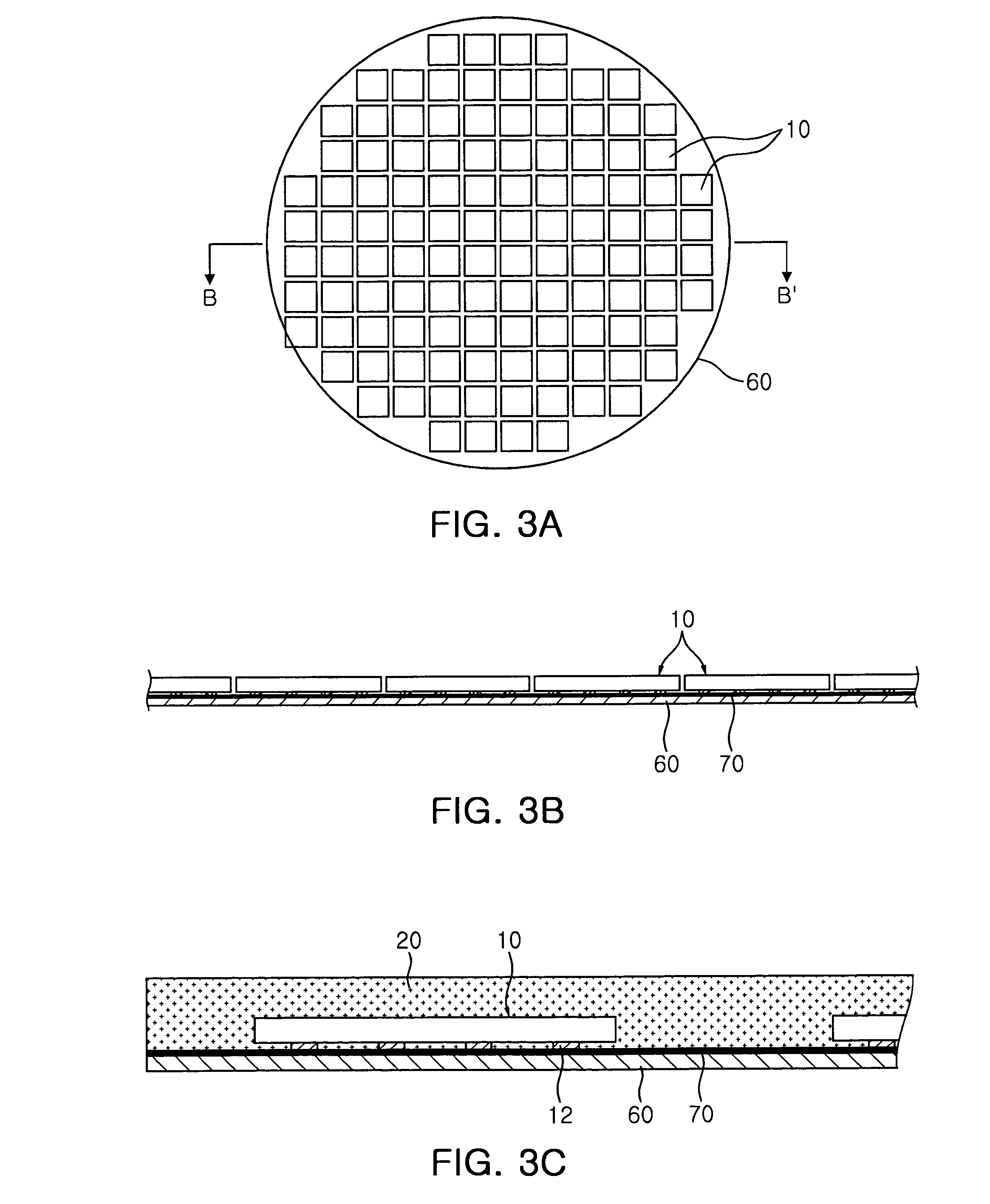
[0040]Prior to a detailed description of the present invention, the terms or words, which are used in the specification and claims to be described below, should not be construed as having typical or dictionary meanings. The terms or words should be construed in conformity with the technical idea of the present invention on the basis of the principle that the inventor(s) can appropriately define terms in order to describe his or her invention in the best way. Embodiments described in the specification and structures illustrated in drawings are merely exemplary embodiments of the present invention. Thus, it is intended that the present invention covers the modifications and variations of this invention, provided they fall within the scope of their equivalents at the time of filing this application.

[0041]Exemplary embodiments of the present invention will be described in detail with reference to the accompanying drawings. The same reference numerals will be used throughout to designate...


PUM


Abstract

There are provided a semiconductor package including an antenna formed integrally therewith, and a method of manufacturing the same. The semiconductor package includes: a semiconductor chip; a sealing part sealing the semiconductor chip; a substrate part formed on at least one surface of the sealing part; and an antenna part formed on the sealing part or the substrate part and electrically connected to the semiconductor chip.

Description

CROSS-REFERENCE TO RELATED APPLICATIONS[0001]This application claims the priority of Korean Patent Application No. 10-2011-0067437 filed on Jul. 7, 2011, in the Korean Intellectual Property Office, the disclosure of which is incorporated herein by reference.BACKGROUND OF THE INVENTION[0002]1. Field of the Invention[0003]The present invention relates to a semiconductor package and a method of manufacturing the same, and more particularly, to a semiconductor package including an antenna formed integrally therewith, and a method of manufacturing the same.[0004]2. Description of the Related Art[0005]As a frequency resource for a next generation information communication service, a frequency in the millimeter wave band, a super high frequency band of 30 GHz or more, has been actively studied.[0006]This frequency in the millimeter wave band has advantages in that a large amount of information may be transferred at high speed using wideband characteristics and that the frequency may be re-...

Claims


Application Information

Patent Timeline
Patent Type & Authority Applications(United States)
IPC IPC(8): H01L23/48H01L21/56
CPCH01L2224/16225H01L24/97H01L2224/73265H01L2224/97H01L2224/32145H01L2224/04105H01L24/19H01L2224/0401H01L2924/3011H01L23/5226H05K2203/061H01L21/565H01L2223/6677H01L25/16H01L25/0657H01L2224/48227H01L2924/01029H01L23/49827H01L21/561H01L21/568H01L23/5389H01L23/66H01L24/96H05K1/185H01L21/56H01L2224/81H01L2924/00H01L2924/00012H01L2924/15787H01L2924/181H01L2924/12042H01L24/73H01L23/12H01Q1/24H01L23/48H01L21/4853H01L21/4857H01L21/486H01L21/78H01L23/3142H01L23/49822H01L23/49838H01L2223/6616H01L2223/6683
Inventor YOO, DO JAEYOON, JUNG HOPARK, CHUL GYUNHAN, MYEONG WOOLEE, JUNG AUN
Owner SAMSUNG ELECTRO MECHANICS CO LTD
Why Eureka
Try Eureka