Composition and method for preparation of organic electronic devices

a technology of electronic devices and organic materials, applied in the direction of sustainable manufacturing/processing, non-metal conductors, final product manufacturing, etc., can solve the problems of difficult production of multi-layer devices based on the technology as mentioned above, drawbacks regarding the performance of films formed, and difficult to achieve high-level film forming, performance, lifetime and efficiency of oe devices can be improved, and the effect of high film forming

Inactive Publication Date: 2013-01-31
MERCK PATENT GMBH
View PDF12 Cites 26 Cited by
  • Summary
  • Abstract
  • Description
  • Claims
  • Application Information

AI Technical Summary

Benefits of technology

[0019]The compositions, methods and devices of the present invention provide surprising improvements in the efficiency of the OE devices and the production thereof. Unexpectedly, the performance, the lifetime and the efficiency of the OE devices can be improved, if these devices are achieved by using a ...

Problems solved by technology

In addition thereto, the formation of films having a high leveling is difficult without the use of high amounts of wetting agents.
However, these wetting agents may have some drawbacks regarding the performance of the films formed.
Furthermore, the production of multilayer devices based on th...

Method used


Image

  • Composition and method for preparation of organic electronic devices
  • Composition and method for preparation of organic electronic devices
  • Composition and method for preparation of organic electronic devices

Examples


example 1

[0216]The substrate (2 cm2 glass plates coated with PEDOT) was activated by heating for 10 minutes at 180° C. and used directly.

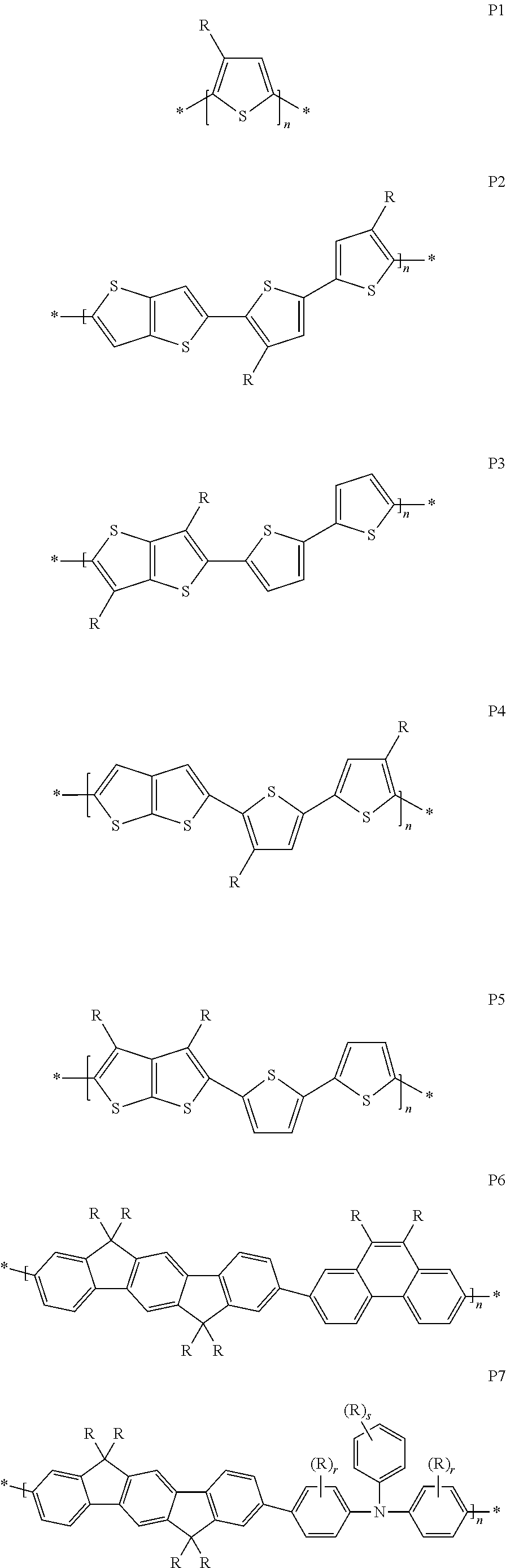
[0217]An OLED polymer ink was formulated by dissolving 0.5% by weight OLED polymer comprising structural units of the following formulae

in a weight ratio of 9% to 11% to 41% to 24% to 5% to 8% to 2% in pentamethylbenzene and gave a viscosity of 3.8 cp at 60° C.

[0218]The ink was printed with the Dimatix DMP 2800 printer (print head heated to 60° C. plus heated glove) onto the substrate. 6 mm squares were printed with a drop spacing of 5, 10, 15, 20, 25, 30, 35 and 40 μm. Drop formation in the ink jet process was good as determined by visualization using a microscope illuminated by a strobe which effectively freezes the droplets in flight.

[0219]After printing the ink on the substrate, further leveling was achieved by heating and cooling the film before removal of the solvent (53° C. for about 20 seconds).

[0220]Thereafter, the solvent was removed on a hot plat...

examples 2 to 4

[0222]Example 1 was repeated. However, 1% OLED polymer as mentioned in Example 1 was dissolved in 2-methylnaphthalene, pentamethylbenzene and 1,5-dimethylnaphthalene by heating the solvent to 80° C., respectively.

[0223]The compositions were processed as described in Example 1. However, the temperature of the leveling step was about 2-5° C. above the melting point of the solvent for approximately 20 seconds and the solvent removal was performed at 100° C.

[0224]Excellent OLED films were formed as observed via a fluorescence method (using a Nikon Eclipse E400 microscope).

example 5

[0225]Example 1 was repeated. However, 1% OLED polymer as mentioned in Example 1 was dissolved in 1,2,4,5-tetramethylbenzene by heating the solvent to 85° C.

[0226]The composition was processed as described in Example 1. However, the temperature of the leveling step was about 88° C. and the solvent removal was performed at 100° C.

[0227]An excellent OLED film was formed as observed via a fluorescence method (using a Nikon Eclipse E400 microscope).


PUM

PropertyMeasurementUnit
Temperatureaaaaaaaaaa

Abstract

The present invention relates to novel compositions comprising an organic semiconductor (OSC) and one or more organic solvents. The composition is solid at a temperature of 25° C. and fluid at a higher temperature and the boiling point of the solvent is at most 400° C. Furthermore, the present invention describes the use of these compositions as inks for the preparation of organic electronic (OE) devices, especially organic photovoltaic (OPV) cells and OLED devices, to methods for preparing OE devices using the novel compositions, and to OE devices, OLED devices and OPV cells prepared from such methods and compositions.

Description

CROSS-REFERENCE TO RELATED APPLICATIONS[0001]This application is a national stage application (under 35 U.S.C. §371) of PCT / EP2011 / 001682, filed Apr. 5, 2011, which claims benefit of European application 10003857.9, filed Apr. 12, 2010.FIELD OF THE INVENTION[0002]The present invention relates to novel compositions comprising an organic semiconducting compound (OSC), to their use as conducting inks for the preparation of organic electronic (OE) devices, especially organic photovoltaic (OPV) cells and OLED devices, to methods for preparing OE devices using the novel formulations, and to OE devices and OPV cells prepared from such methods and compositions.BACKGROUND AND PRIOR ART[0003]When preparing OE devices like OFETs or OPV cells, in particular flexible devices, usually printing or coating techniques like inkjet printing, roll to roll printing, slot dye coating or flexographic / gravure printing are used to apply the OSC layer. Based on low solubility of the most of the present organ...

Claims


Application Information

Patent Timeline
IPC IPC(8): H01B1/12H01L51/00C09D11/02
CPCH01L51/0005H01L51/0007H01L51/0035H01L51/0037H01L51/0043H01L51/0052Y02E10/549H01L51/0085H01L51/0094H01L51/0541H01L51/0545H01L51/5012H01L51/5016H01L51/0074C09D5/22C09K11/025C09K11/06Y02P70/50H10K71/135H10K71/15H10K85/111H10K85/1135H10K85/151H10K85/615H10K85/6576H10K85/342H10K85/40H10K10/464H10K10/466H10K50/11H10K2101/10C08G61/12H10K85/115H10K85/624H10K85/626H10K10/488H10K30/30H10K71/12H10K71/13C08G61/123C08G2261/124C08G2261/228C08G2261/312C08G2261/314C08G2261/3142C08G2261/3162C08G2261/3223C08G2261/91C08G2261/92C08G2261/95C09D5/24C09D165/00C09K2211/1416C09K2211/1425C09K2211/1433C09K2211/1458
Inventor JAMES, MARKGONCALVES-MISKIEWICZ, MAGDAMAY, PHILIP EDWARDNANSON, LANAEFFENBERGER, RUTHKLUGE, EDGAR
Owner MERCK PATENT GMBH
Why Eureka
Try Eureka