Silicon light emitting device and method of fabricating same

a technology of light-emitting devices and silicon, which is applied in the direction of semiconductor/solid-state device manufacturing, semiconductor/conductor devices, electrical devices, etc., can solve the problems of barriers formed between mutually facing faces

Active Publication Date: 2013-01-31
INSIAVA
View PDF3 Cites 20 Cited by
  • Summary
  • Abstract
  • Description
  • Claims
  • Application Information

AI Technical Summary

Problems solved by technology

These techniques, by necessity, cause the barriers to be for...

Method used


Image

  • Silicon light emitting device and method of fabricating same
  • Silicon light emitting device and method of fabricating same
  • Silicon light emitting device and method of fabricating same

Examples


Embodiment Construction

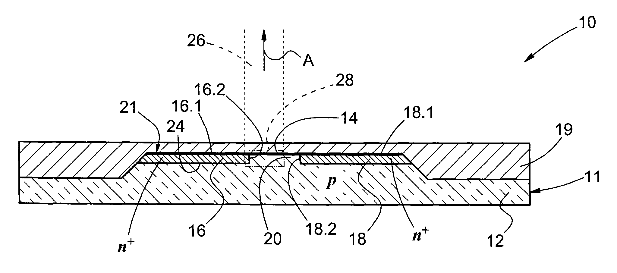
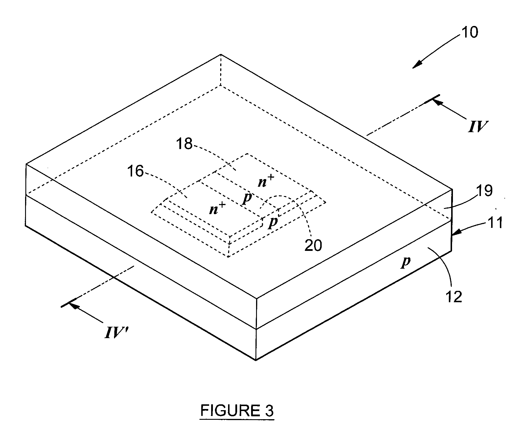
[0040]A light emitting device according to the invention is generally designated by the reference numeral 10 in FIGS. 3 and 4.

[0041]The light emitting device 10 comprises a body 11 comprising a substrate 12 of a semiconductor material. In the example embodiment shown, an indirect bandgap semiconductor material, in the form of silicon, of a first doping kind p and a first doping concentration is used. The substrate has an upper surface 14. A first island 16 of a second doping kind and a second doping concentration n+ and a second island 18 of a third doping kind and a third doping concentration (in this case also n+) are formed on one side of the upper surface 14 of the substrate 12 according to a standard bulk semiconductor fabrication process (such as a standard sub-micron process, such as a standard 0.35 μm CMOS process) utilizing lateral device isolation techniques utilizing lateral active area physical isolation (such as LOCOS or STI). The first island is embedded in the substra...


PUM


Abstract

A light emitting device (10) comprises a body (11) comprising a substrate (12) of a p-type semiconductor material. The substrate has an upper surface (14) and having formed therein on one side of the upper surface and according to a bulk semi-conductor fabrication process utilizing lateral active area isolation techniques: a first n+-type island (16) to form a first junction (24) between the first island and the substrate; and a second n+-type island (18) spaced laterally from the first island (16). The substrate provides a laterally extending link (20) between the islands having an upper surface. The upper surface of the link, an upper surface of the island (16) and an upper surface of the island (18) collectively form a planar interface (21) between the body (11) and an isolation layer (19) of the device. The device comprises a terminal arrangement to apply a reverse bias to the first junction, to cause the device to emit light. The device is configured to facilitate the transmission of the emitted light.

Description

INTRODUCTION AND BACKGROUND[0001]This invention relates to optoelectronic devices and more particularly to light emitting devices fabricated from a semiconductor material, such as silicon, and a method of fabricating such a device.[0002]Light emitting devices fabricated from silicon are known in the art. One such a device is a two junction device having a sandwiched configuration of immediately adjacent doped p+np+ or n+pn+ regions. The device comprises a first pn junction which is reverse biased into a breakdown mode, to emit light and a neighbouring second pn junction which is forward biased to inject carriers into the first junction, thereby to improve the internal quantum efficiency of the device. It is also known to drive the device into a punch-through mode wherein a depletion region associated with the reverse biased junction punches through to a depletion region associated with the forward biased junction, thereby to lower an energy barrier of the forward biased junction and...

Claims


Application Information

Patent Timeline
IPC IPC(8): H01L33/00
CPCH01L33/34H01L33/0016
Inventor VENTER, PETRUS JOHANNES
Owner INSIAVA
Why Eureka
Try Eureka