Charge-sharing path control device for a scan driver of an LCD panel

Active Publication Date: 2013-01-31
STMICROELECTRONICS SRL
View PDF11 Cites 11 Cited by
  • Summary
  • Abstract
  • Description
  • Claims
  • Application Information

AI Technical Summary

Benefits of technology

The patent describes a technology that allows for efficient and safe transfer of electrical charges in both directions. This is achieved through a single controlled charge transfer path, which can be activated and deactivated to transfer charges between different channels or nodes. The technology also includes clamps and resistors to protect the circuit and ensure efficient charge recycling. Overall, the technology reduces the biasing current required for a full charge sharing and utilizes a latched structure to achieve better charge transfer control.

Problems solved by technology

With this trend, power dissipation, which is also tied to the size of the displays, is a serious concern.
As a result, scan driver design is becoming more and more challenging.
The charge sharing function is limited to a sharing between complementary outputs, and availability of relatively high voltage zener diodes in the silicon fabrication technology is required.
The approach is not applicable to GOA panels because of the relatively high voltage rails required with this LCD technology for correct driving of the gate lines.
Even a hypothetical implementation of the disclosed circuits with high voltage MOSFETs would not work because of the presence of an intrinsic diode between the source and drain that could provide an undesirable discharge path to the channels during a charge sharing phase.

Method used


Image

  • Charge-sharing path control device for a scan driver of an LCD panel
  • Charge-sharing path control device for a scan driver of an LCD panel
  • Charge-sharing path control device for a scan driver of an LCD panel

Examples


Embodiment Construction

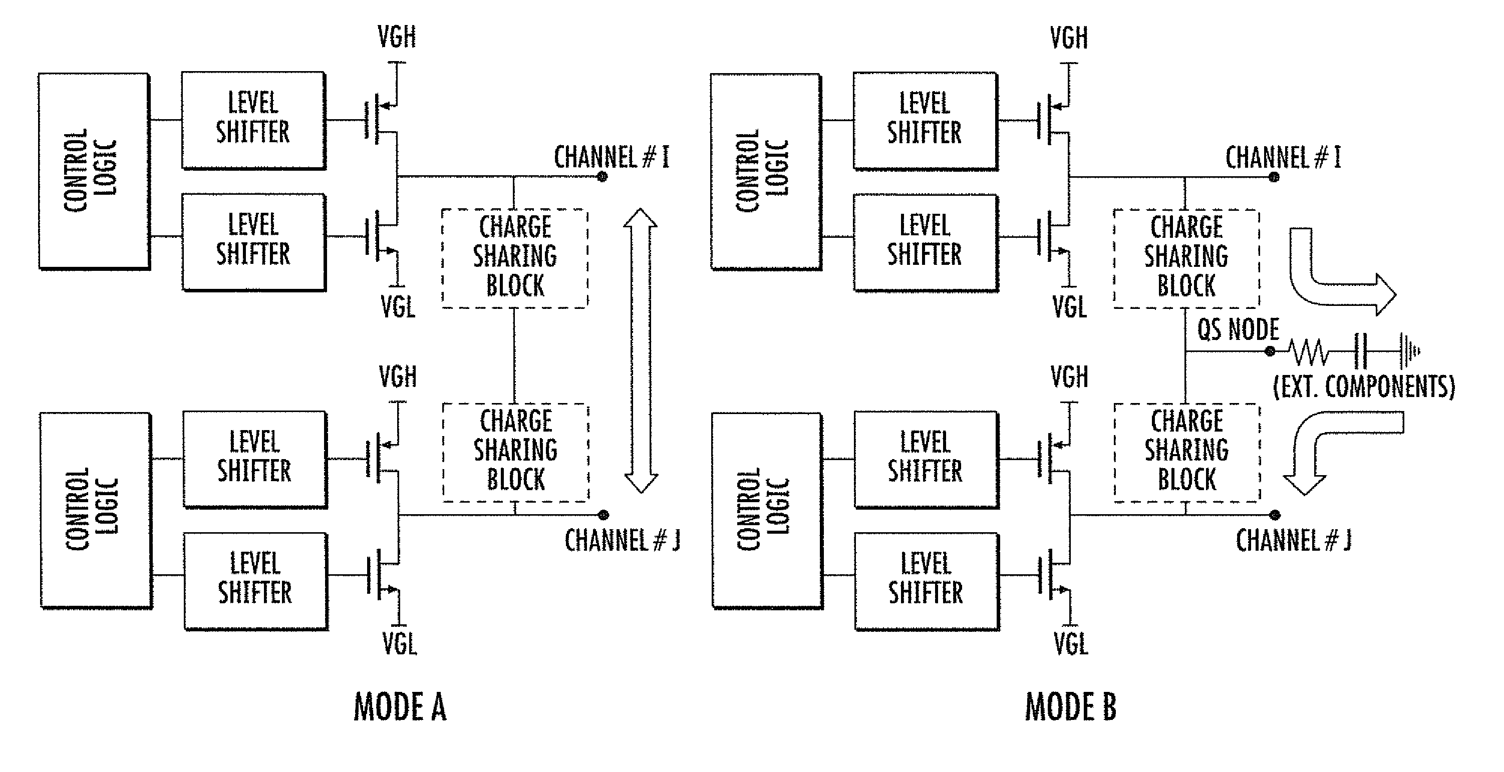
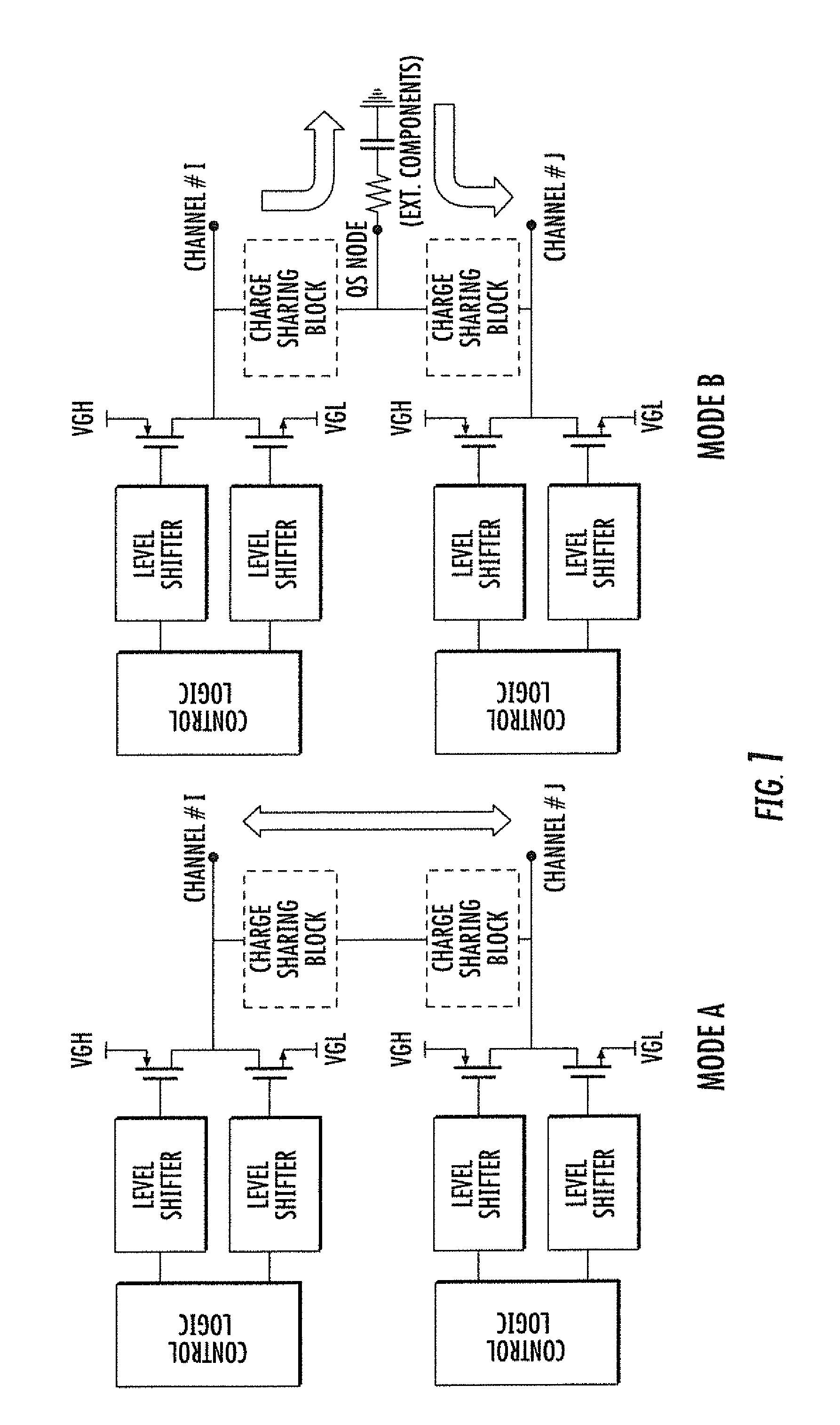
[0021]The basic functional block diagrams of FIG. 1 represent the same level-shifter-output-buffer block diagram of a scan driver for an LCD panel, including functional circuitry, depicted by the shaded blocks, for implementing a charge sharing function according to two different operating modes.

[0022]According to a Mode A implementation, charge sharing occurs between adjacent scan channels sequentially activated by the scan driver. According to the Mode B implementation, charge sharing occurs through a charge storage node QS. This is other than a total capacitance associated with an adjacent channel, which is typically an externally connected capacitor. The bidirectional single path charge sharing device supports both modes of implementation of the charge sharing function.

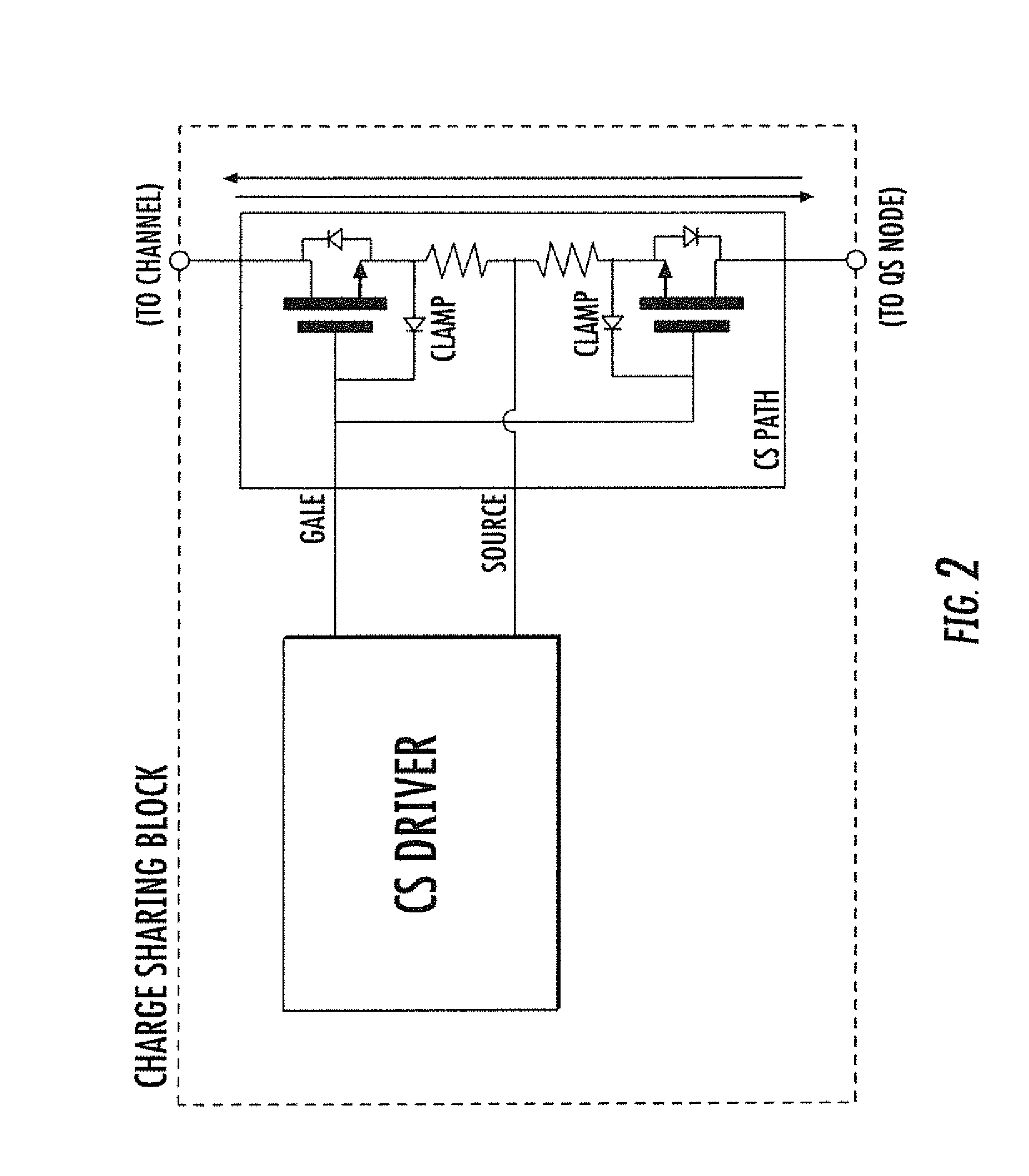
[0023]FIG. 2 is a basic illustration of an exemplary embodiment of a bidirectional switch used in the bidirectional single path charge sharing device as discussed herein. According to this embodiment, the bidirect...


PUM

PropertyMeasurementUnit
Electrical resistanceaaaaaaaaaa
Charge transfer stateaaaaaaaaaa

Abstract

A bidirectional switch includes a pair of transistors, with each transistor including a source connected via a degeneration resistance to a common source control node, a gate connected to a common gate control node, a drain connected to a respective channel or gate line and to a charge storage node, respectively, and a clamp diode connected between the source and the gate. This forms a single charge transfer path between gate lines sequentially activated by a scan driver of an LCD panel, and implements a charge sharing technique for reducing power dissipation.

Description

FIELD OF THE INVENTION[0001]The present invention relates in general to LCD panels with reduced power dissipation, and in particular, to a bidirectional single path charge sharing switching device in a scan driver configured to scan numerous channels (gate lines) in sequence with reduced power dissipation.BACKGROUND OF THE INVENTION[0002]In current display panels, the scanning frequency is ever increasing to support high definition image frame rates, especially for 3D image visualization, where the frame rate is double compared to the equivalent 2D visualization. With this trend, power dissipation, which is also tied to the size of the displays, is a serious concern. As a result, scan driver design is becoming more and more challenging.[0003]Charge sharing techniques have been developed, and are being implemented by major panel manufacturers. The charge sharing method reuses (recycles) part of the electrical charge accumulated in the activated, commonly buffered, channel or gate lin...

Claims


Application Information

Patent Timeline
IPC IPC(8): G09G3/36H01H11/00
CPCG09G2330/023Y10T29/49105G09G3/3674
Inventor CRISTAUDO, DOMENICOCORRADI, STEFANOSUERI, STEFANO
Owner STMICROELECTRONICS SRL
Why Eureka
Try Eureka