Electro-optical device, method of driving electro-optical device, electronic apparatus, and projector

a technology of electrooptical devices and electrooptical devices, applied in the direction of electric digital data processing, instruments, computing, etc., can solve problems such as image sticking (spots and unevenness) in liquid crystal devices, and achieve the effect of reducing the amount of leakage light of preventing the decrease of the contrast caused by the ion trap section, and raising the trapping voltag

Inactive Publication Date: 2013-01-31
SEIKO EPSON CORP
View PDF4 Cites 12 Cited by
  • Summary
  • Abstract
  • Description
  • Claims
  • Application Information

AI Technical Summary

Benefits of technology

[0018]With this driving method, a high trapping voltage is applied to the ion trap section when the driving voltage of the pixel is high, and a low trapping voltage is applied when the driving voltage of the pixel is low. The amount of leakage light of the ion trap section can therefore be decreased when a dark image is displayed in the pixel region, so that a decrease in contrast caused by the ion trap section can be prevented. Moreover, the trapping voltage is raised when a bright image, with which leakage light hardly influences contrast, is displayed. The trap efficiency of the ion trap section will not be excessively reduced.
[0019]An electronic apparatus according to a third aspect of the invention includes the above electro-optical device. With this configuration, the electronic apparatus including an optical modulation unit

Problems solved by technology

It is known that ionic contamination in a liquid crystal layer caus

Method used


Image

  • Electro-optical device, method of driving electro-optical device, electronic apparatus, and projector
  • Electro-optical device, method of driving electro-optical device, electronic apparatus, and projector
  • Electro-optical device, method of driving electro-optical device, electronic apparatus, and projector

Examples


first embodiment

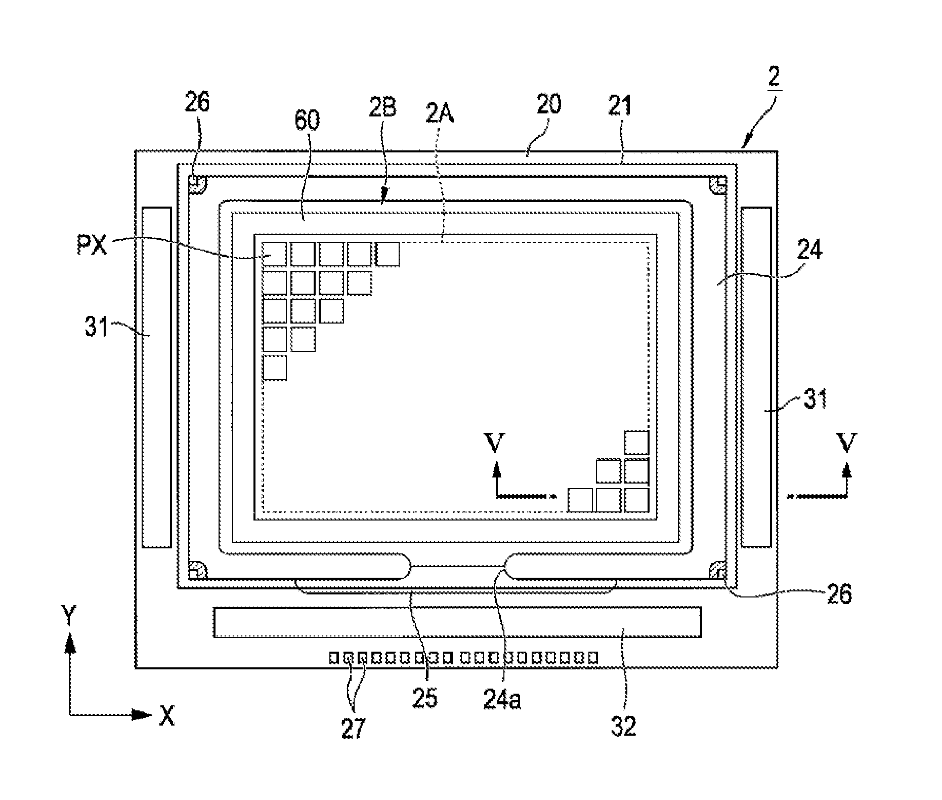
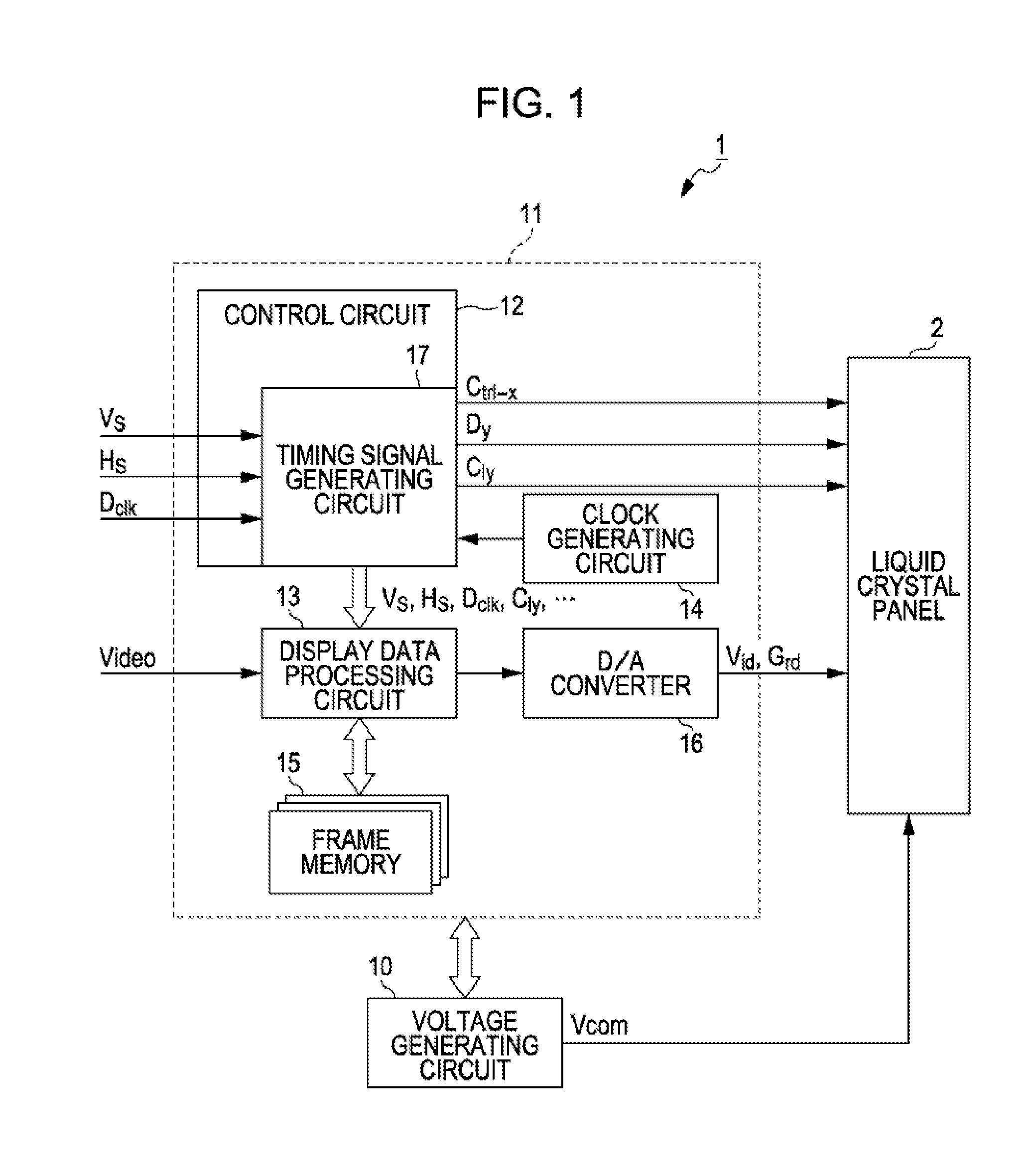
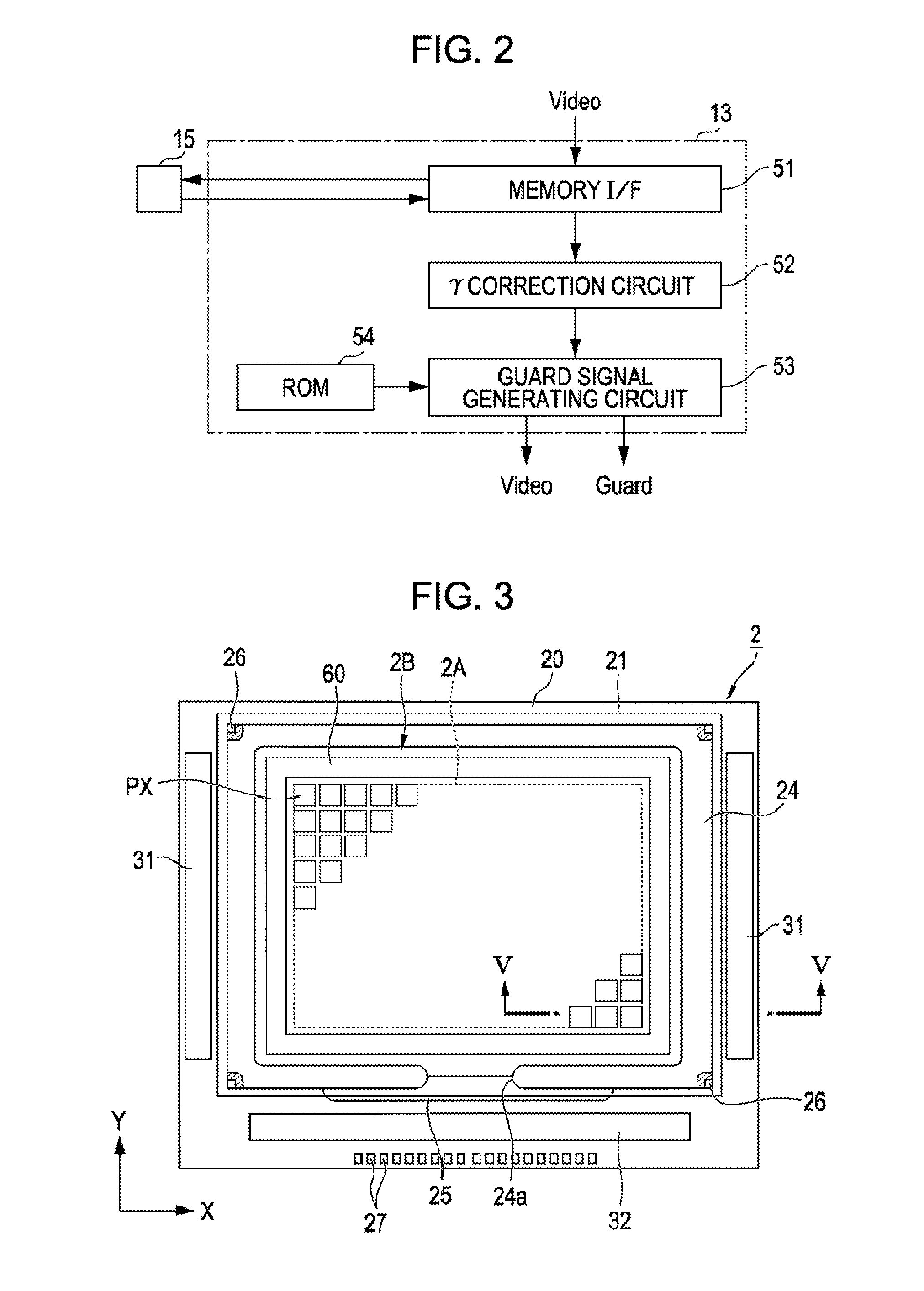
[0033]FIG. 1 is a block diagram illustrating a schematic configuration of a liquid crystal device according to a first embodiment. FIG. 2 is a block diagram illustrating a configuration of a display data processing circuit. FIG. 3 is a plan view illustrating a schematic configuration of a liquid crystal panel. FIG. 4 illustrates a circuit configuration of the liquid crystal panel.

[0034]A liquid crystal device (electro-optical device) 1 illustrated in FIG. 1 includes a liquid crystal panel 2, a voltage generating circuit 10, and a control device 11. The liquid crystal panel 2 is an active-matrix driven reflection-type liquid crystal panel, for example, and the detailed configuration thereof will be described later.

[0035]The voltage generating circuit 10 includes a DC to DC converter or the like. The voltage generating circuit 10 generates direct-current (DC) voltages of a plurality of levels, which are to be used in components of the liquid crystal device 1, under control of the cont...

second embodiment

[0085]With reference to FIGS. 7A and 7B, a second embodiment will be described next. This embodiment is an example in which operations of the display data processing circuit 13 in the liquid crystal device 1 are changed from those in the first embodiment. FIGS. 7A and 7B are explanatory diagrams of operations of a liquid crystal device according to the second embodiment. FIG. 7A is a graph schematically representing the time variation of the average value of driving voltage input to the pixel electrode 35 of the pixel PX in an image display operation of the liquid crystal panel 2. FIG. 7B is a graph schematically representing the time variation of the trapping voltage input to the trapping electrode 61 of the ion trap section 60. The vertical axes of the graphs illustrated in FIGS. 7A and 7B represent the voltage (V), and the horizontal axes represent time (msec).

[0086]As illustrated in FIG. 7B, the trapping voltage applied to the trapping electrode 61 is a DC voltage in the driving...

third embodiment

[0089]With reference to FIGS. 8A and 8B, a third embodiment will be described next. This embodiment is an example in which operations of the display data processing circuit 13 in the liquid crystal device 1 are changed from those in the first embodiment. FIGS. 8A and 8B are explanatory diagrams of operations of a liquid crystal device according to the third embodiment. FIG. 8A is a graph schematically representing the time variation of the average value of driving voltage input to the pixel electrode 35 of the pixel PX in an image display operation of the liquid crystal panel 2. FIG. 8B is a graph schematically representing the time variation of the trapping voltage input to the trapping electrode 61 of the ion trap section 60. The vertical axes of the graphs illustrated in FIGS. 8A and 8B represent the voltage (V), and the horizontal axes represent time (msec).

[0090]As illustrated in FIG. 8B, in the driving method of this embodiment, the trapping voltage applied to the trapping ele...


PUM


Abstract

An electro-optical device of the invention includes a first substrate and a second substrate facing each other with an electro-optical medium sandwiched therebetween, a pixel region having a plurality of pixels, and an ion trap section having an electrode formed in a region outside of the pixel region. A trapping voltage applied to the electrode of the ion trap section varies in accordance with a calculated voltage value that is calculated from a driving voltage applied to the electro-optical medium in one or a plurality of the pixels serving as a reference. The trapping voltage is set relatively high when the calculated voltage value belongs to a relatively high voltage range, and the trapping voltage is set relatively low when the calculated voltage value belongs to a relatively low voltage range.

Description

BACKGROUND[0001]1. Technical Field[0002]The present invention relates to an electro-optical device, a method of driving the electro-optical device, an electronic apparatus, and a projector.[0003]2. Related Art[0004]It is known that ionic contamination in a liquid crystal layer causes image sticking (spots and unevenness) in a liquid crystal device. To address this issue, there have been proposals for a plurality of electrodes to be formed in a peripheral region outside of a pixel region, and a voltage is applied across the plurality of electrodes, thereby causing ionic impurities to be adsorbed to the peripheral region (see, for example, JP-A-2007-316119 and JP-A-2007-249105).[0005]In the above ion trap section having a plurality of electrodes, a voltage at least sufficient to cause a response in liquid crystal needs to be applied to the plurality of electrodes in order to trap ionic impurities in a liquid crystal layer. However, when liquid crystal responds in the region in which t...

Claims


Application Information

Patent Timeline
IPC IPC(8): G02F1/1333G09G5/02G02F1/13357G09G3/36
CPCG09G3/2092G09G3/3648G09G2310/0232G02F2201/50G09G2320/0276G02F2001/133337G02F2201/122G09G2320/0238G02F1/133337
Inventor NISHIDA, MASAKAZUSAWADO, AYAE
Owner SEIKO EPSON CORP
Why Eureka
Try Eureka