Optical element, light source device, and projection display device

a technology of optical elements and light sources, applied in non-linear optics, lighting and heating apparatus, instruments, etc., can solve the problems of increasing the etendue of the light source itself, increasing the light-emitting area of the entire light source, etc., and achieve the effect of reducing the etendue of the light from the optical elemen

Active Publication Date: 2013-02-07
NEC CORP
View PDF4 Cites 19 Cited by
  • Summary
  • Abstract
  • Description
  • Claims
  • Application Information

AI Technical Summary

Benefits of technology

[0021]According to the present invention, the etendue of the light from the optical element can be reduced without any dependence on the etendue of the light-emitting element.

Problems solved by technology

In the configuration described in Patent Literature 2, the arrangement of the plurality of LEDs 300 on the plane causes an increase of the light-emitting area of the entire light source, and thus a problem arises in which there is an increase in the etendue of the light source itself.

Method used


Image

  • Optical element, light source device, and projection display device
  • Optical element, light source device, and projection display device
  • Optical element, light source device, and projection display device

Examples


first embodiment

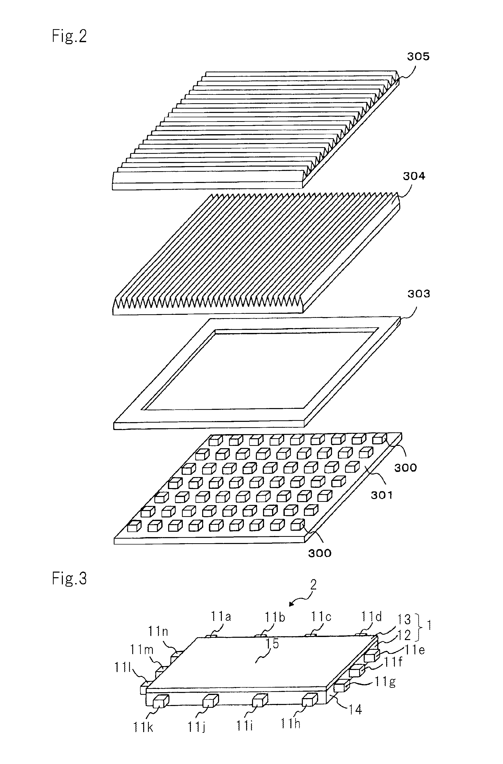
[0054]FIG. 3 is a schematic perspective view showing a configuration of a light source device according to a first embodiment. FIG. 4 is an explanatory sectional view showing behavior of light in the light source device according to the present invention. In the light source device, individual layers actually have very large thicknesses, and there is a large difference in thickness among the layers. It is therefore difficult to draw the layers in accurate scale and proportion. Thus, in the drawings, the layers are not drawn in actual proportion, and hence are schematically shown.

[0055]As shown in FIGS. 3 and 4, light source device 2 according to the present embodiment includes a plurality of light-emitting elements 11 (11a to 11n) and optical element 1 into which lights output from light-emitting elements 11 enter. Optical element 1 includes light guide body 12 into which the lights output from light-emitting elements 11 enter, and directional control layer 13 for emitting output li...

second embodiment

[0084]For wave vector conversion layer 18, in place of a photonic crystal, a configuration where a microlens array is disposed, or a configuration using a layer having a rough surface can be used. FIG. 7 is a perspective view schematically showing a directional control layer included in a light source device according to a second embodiment.

[0085]As shown in FIG. 7, in directional control layer 23, wave vector conversion layer 28 including a microlens array is disposed on the surface of plasmon excitation layer 17. Even in the configuration that includes wave vector conversion layer 28 including a microlens array, directional control layer 23 can provide the same effects as those in the configuration that includes wave vector conversion layer 18 made of the photonic crystal.

[0086]FIGS. 8A and 8B are explanatory sectional views showing the manufacturing process of a configuration where the microlens array is stacked on plasmon excitation layer 17. In the configuration including the m...
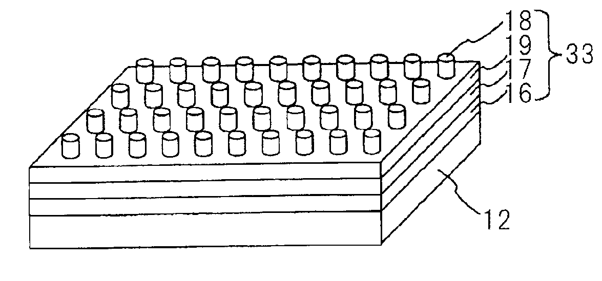
third embodiment

[0090]FIG. 9 is a perspective view showing a directional control layer included in a light source device according to a third embodiment. As shown in FIG. 9, in directional control layer 33 according to the third embodiment, carrier generation layer 16, plasmon excitation layer 17, dielectric constant layer 19, and wave vector conversion layer 18 are stacked in order on light guide body 12.

[0091]Thus, the third embodiment is different from the first embodiment in that dielectric constant layer 19 is independently disposed between plasmon excitation layer 17 and wave vector conversion layer 18. Dielectric constant layer 19 has a dielectric constant set lower than that of dielectric constant layer 20 (high dielectric constant layer 20) in a fourth embodiment described below, and thus will be referred to as low dielectric constant layer 19. For the dielectric constant of low dielectric constant layer 19, a range where the effective dielectric constant of the exit side portion is mainta...


PUM

PropertyMeasurementUnit
thicknessaaaaaaaaaa
thicknessaaaaaaaaaa
thicknessaaaaaaaaaa

Abstract

Disclosed is an optical element that includes: carrier generation layer (16) in which carriers are generated by light from light guide body (12) into which light from a light-emitting element enters; plasmon excitation layer (17) that has a plasma frequency higher than the frequency of light generated when carrier generation layer (16) is excited by light from the light-emitting element; and wave vector conversion layer (18) that converts surface plasmon generated by plasmon excitation layer (17) light having a predetermined exit angle to output the light. Plasmon excitation layer (17) is sandwiched between two layers having dielectric properties. The effective dielectric constant of the incident side portion of plasmon excitation layer (17) including an entire structure stacked above light guide body (12) side is higher than that of the exit side portion of plasmon excitation layer (17) including the entire structure stacked above wave vector conversion layer (18) side and the medium in contact with wave vector conversion layer (18).

Description

TECHNICAL FIELD[0001]The present invention relates to an optical element that uses surface plasmon to output light, a light source device, and a projection display device.BACKGROUND ART[0002]There has been proposed a light-emitting diode (LED) projector that uses a LED as a light-emitting element included in the light source device. The LED projector of this type includes a light source device having a LED, an illumination optical system into which light from the light source device enters, a light valve having a liquid crystal display plate into which light from the illumination optical system enters, and a projection optical system for projecting light from the light valve to a projection surface.[0003]In the LED projector, to increase the luminance of a projected image, light loss must be prevented as much as possible on an optical path from the light source device to the light valve.[0004]As described in Nonpatent Literature 1, there are restrictions based on etendue that are de...

Claims


Application Information

Patent Timeline
Patent Type & Authority Applications(United States)
IPC IPC(8): G02F1/01F21V9/14G03B21/14F21V8/00
CPCG02B6/005B82Y20/00
Inventor NATSUMEDA, MASANAOIMAI, MASAOSAITOH, GOROHTOMINAGA, SHIN
Owner NEC CORP
Why Eureka
Try Eureka