

Method for allocating addresses to data buffers in distributed buffer chipset
a distributed buffer and address allocation technology, applied in memory adressing/allocation/relocation, digital storage, instruments, etc., can solve the problems of reducing signal integrity, address pins undoubtedly increasing the entire size of the chip, and the maximum memory capacity reaching a limi
- Summary
- Abstract
- Description
- Claims
- Application Information
AI Technical Summary
Benefits of technology
Problems solved by technology
Method used
Image

Examples
first embodiment
The First Embodiment
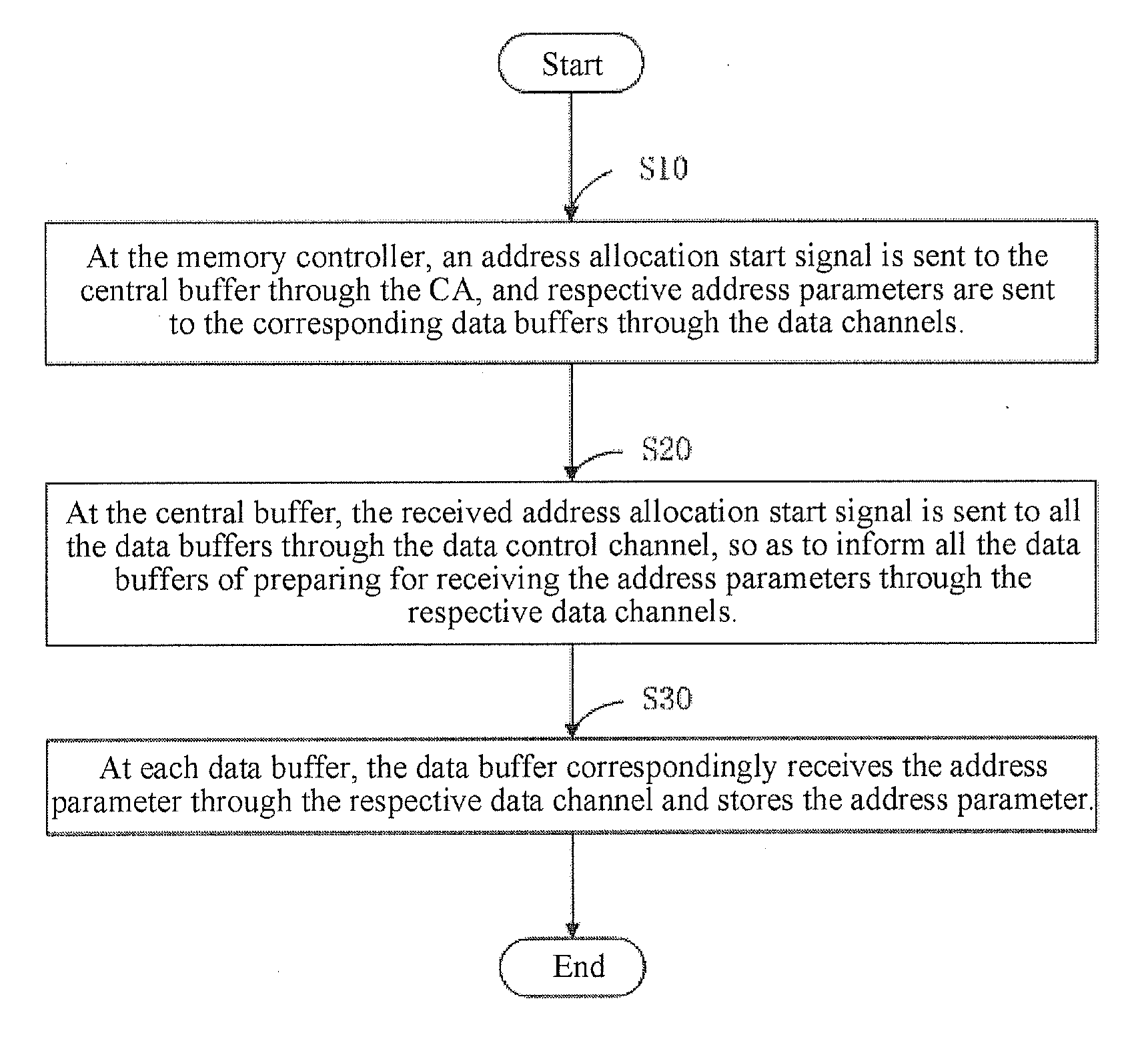
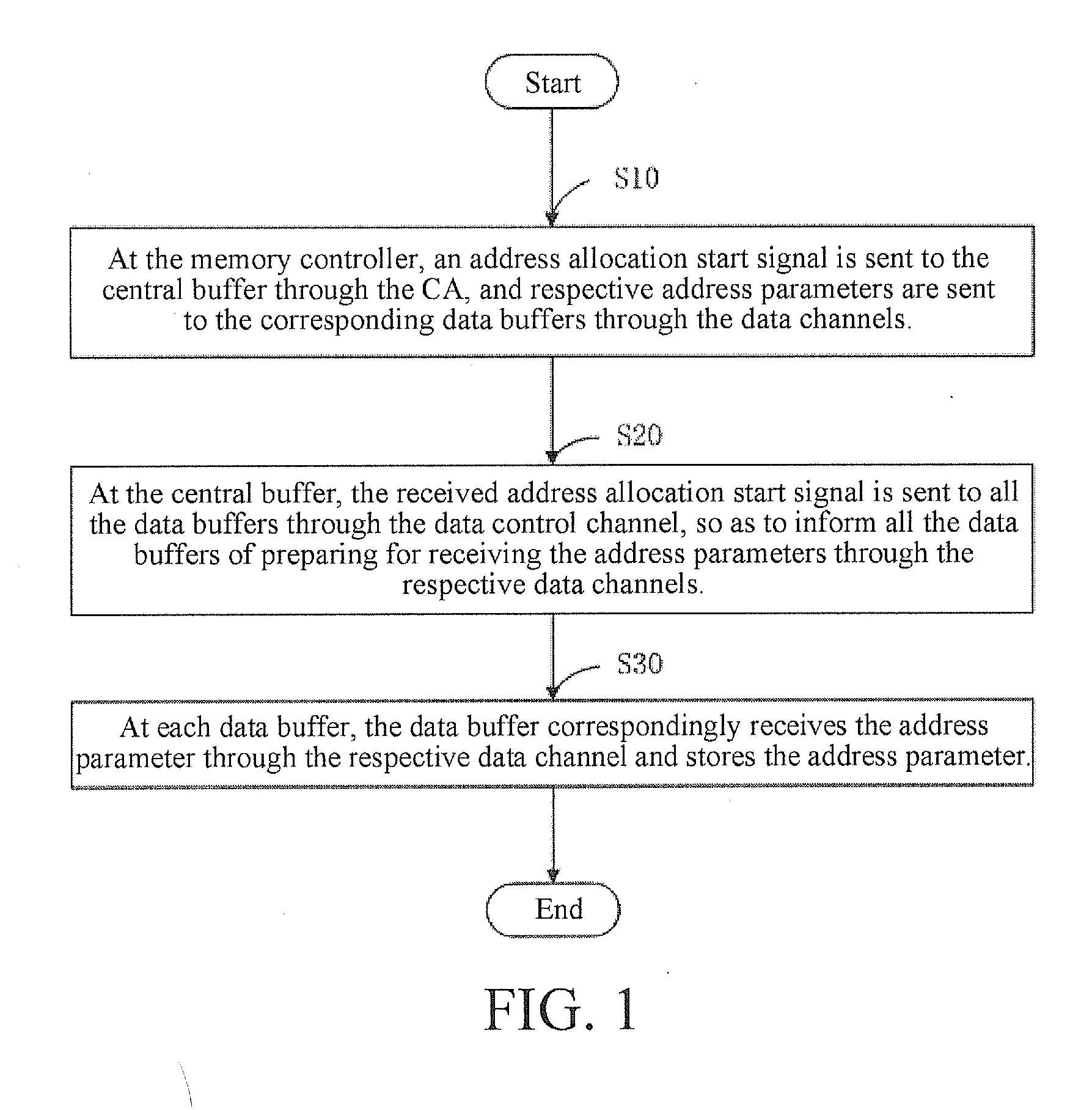
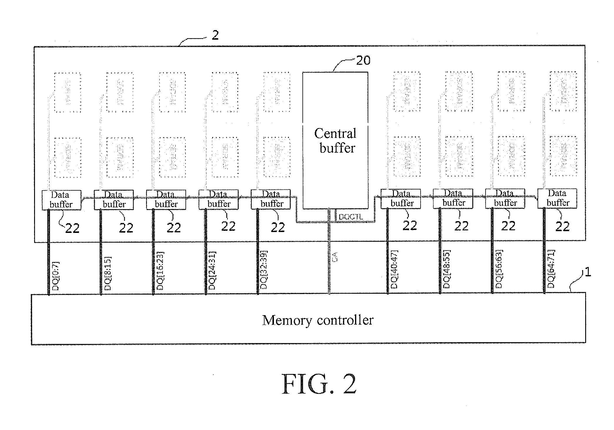
[0040]Preferable, as shown in FIG. 3, is a schematic operational flow chart of a method for allocating addresses to data buffers in a distributed buffer chipset according to the first embodiment of the present invention. The specific operational steps of the method for allocating addresses to data buffers in a distributed buffer chipset in the present invention are described in detail in the following with reference to FIG. 2.
[0041]Step S100 is first performed, in which at the memory controller 1, designated time and a specific number are preset. The designated time is set to ensure that the data buffer 22 has enough time to receive and latch the address configuration value after receiving the address allocation start signal. Then, Step S101 is performed.
[0042]In Step S101, at the memory controller 1, an address allocation start signal is sent to the central buffer 20 through the CA, the time is reset and started, respective address configuration values are sent ...
second embodiment
The Second Embodiment
[0052]FIG. 4 is a schematic operational flow chart of a method for allocating addresses to data buffers in a distributed buffer chipset according to the second embodiment of the present invention. Referring to FIG. 4, steps same as or similar to the steps of the method for allocating addresses to data buffers in a distributed buffer chipset in the above embodiment (as shown in FIG. 3) are indicated by the same or similar symbols, and the detailed description is omitted, so that the description of the present invention is more clear and understandable.
[0053]The major difference between the method for allocating addresses to data buffers in a distributed buffer chipset in the second embodiment and that in the first embodiment lies in that, in the method for allocating addresses to data buffers in a distributed buffer chipset in the first embodiment, each state of sending the address configuration value is maintained for designated time at the memory controller, so...
third embodiment
The Third Embodiment
[0054]FIG. 5 is a schematic operational flow chart of a method for allocating addresses to data buffers in a distributed buffer chipset according to the third embodiment of the present invention. Referring to FIG. 5, steps same as or similar to the steps of the method for allocating addresses to data buffers in a distributed buffer chipset in the above embodiments (as shown in FIG. 3 and FIG. 4) are indicated by the same or similar symbols, and the detailed description is omitted, so that the description of the present invention is more clear and understandable.
[0055]The major difference between the method for allocating addresses to data buffers in a distributed buffer chipset in the third embodiment and that in the first embodiment as well as that in the second embodiment lies in that, in the method for allocating addresses to data buffers in a distributed buffer chipset in the first and the second embodiment, the specific number is used as a cycle index for ad...
PUM
 Abstract
Description
Claims
Application Information