

Light-Emitting Device
a technology of light-emitting devices and light-emitting materials, which is applied in the direction of semiconductor devices, semiconductor/solid-state device details, electrical devices, etc., can solve the problems of loss of hermeticity, difficult optimization of frit material material material, and inability to prevent cracks easily, so as to achieve high reliability and less cracks
- Summary
- Abstract
- Description
- Claims
- Application Information
AI Technical Summary
Benefits of technology
Problems solved by technology
Method used
Image

Examples
embodiment 1
[0044]In this embodiment, examples of the structure of the light-emitting device of an embodiment of the present invention will be described with reference to FIGS. 1A to 1C, FIGS. 2A to 2D, and FIGS. 3A to 3C.
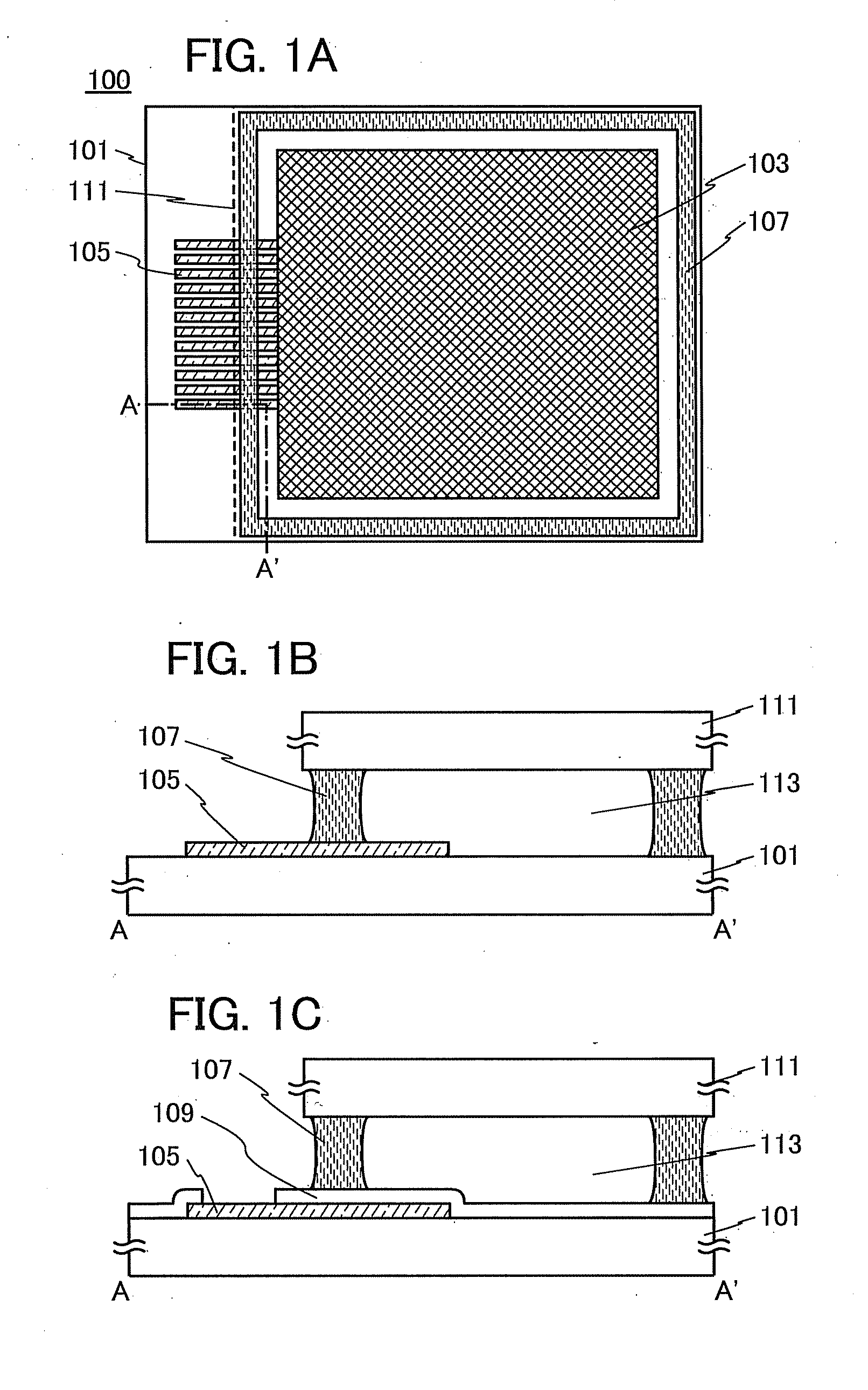
[0045]FIG. 1A is a schematic top view of a light-emitting device 100 shown in this embodiment. FIG. 1B is a schematic cross-sectional view along line A-A′ of FIG. 1A.
[0046]In the light-emitting device 100, a first substrate 101 and a second substrate 111 are bonded to each other to be sealed with a sealing material 107 along the edge of the second substrate 111. Accordingly, the light-emitting device 100 includes a hermetically sealed region 113 which is surrounded by the first substrate 101, the second substrate 111, and the sealing material 107.
[0047]The light-emitting device 100 includes a light-emitting unit 103 in the sealed region 113. As the light-emitting unit 103, an image display device using an organic EL element, a light source, or the like can be used. Examples of...
embodiment 2
[0079]In this embodiment, an example of a structure of a display device will be described with reference to FIGS. 4A and 4B and FIGS. 5A and 5B. In the display device, an image display device combining a thin film transistor and an organic EL element is used as the light-emitting unit shown in Embodiment 1.
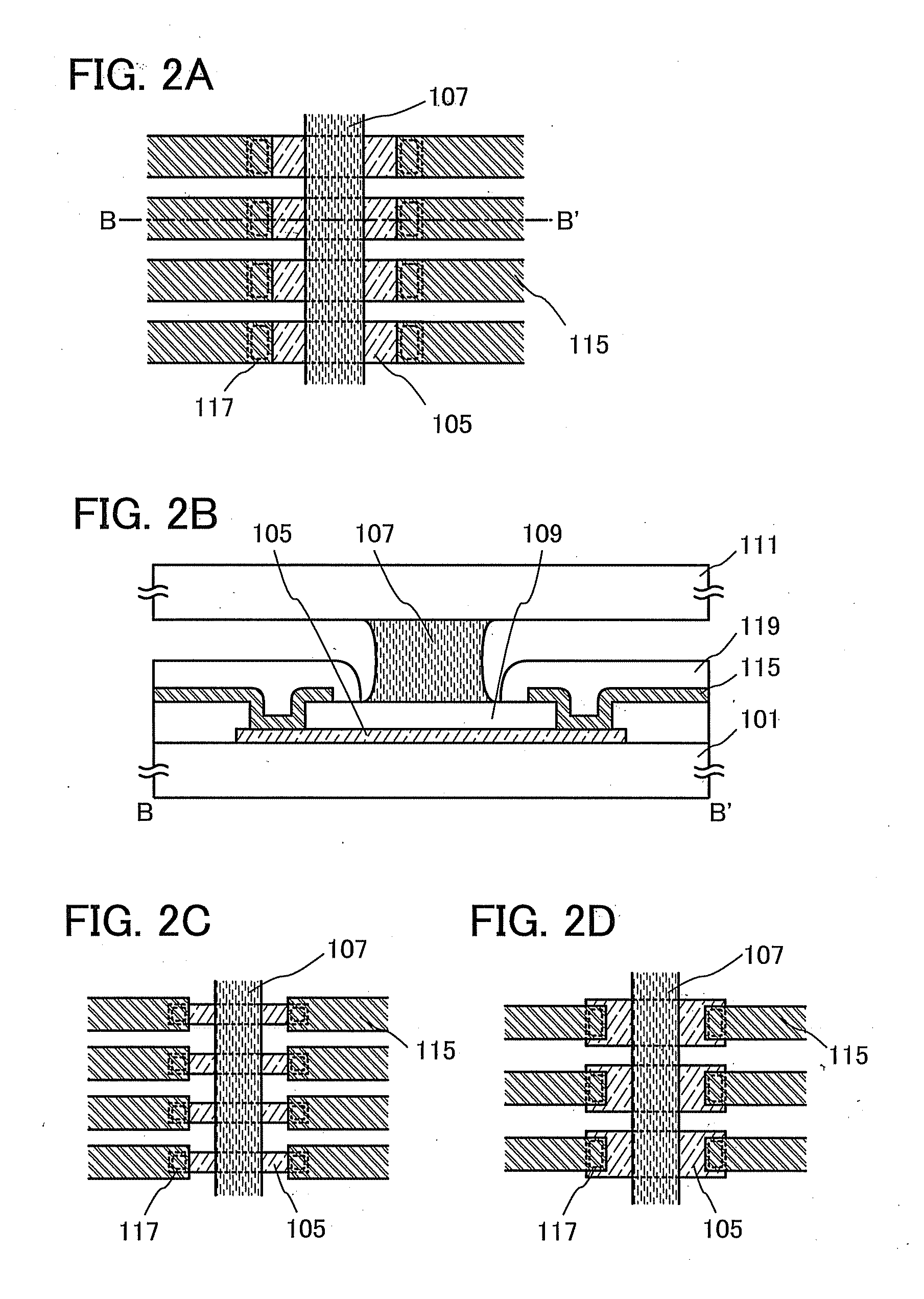
[0080]FIG. 4A is a schematic top view of a display device 200 shown in this embodiment. In the display device 200, the first substrate 101 and the second substrate 111 are bonded to each other to be sealed with the sealing material 107, whereby the hermetically sealed region 113 shown FIG. 4B is formed. In the sealed region 113, a pixel portion 201 including a plurality of pixels and a driver circuit portion 203 driving the pixel portion 201 are formed over the first substrate 101. The display device 200 also includes the plurality of wirings 105 which are electrically connected to the driver circuit portion 203 and extend from the sealed region 113 to the outside of the sealed re...
embodiment 3
[0111]In this embodiment, an example of a lighting device will be described with reference to FIGS. 6A and 6B. In the lighting device, a light source including an organic EL element is used as the light-emitting unit shown in Embodiment 1.
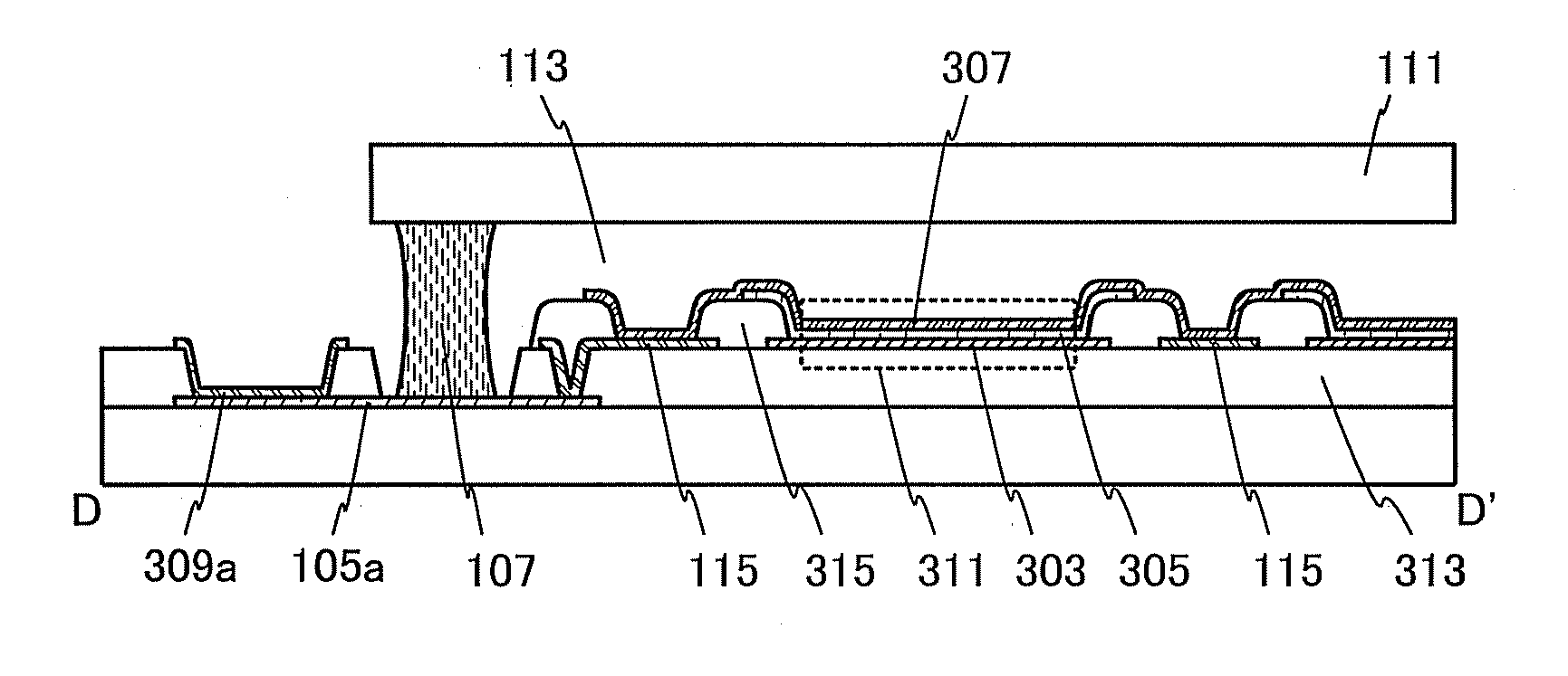
[0112]FIG. 6A is a schematic top view of a lighting device 300 shown in this embodiment. Note that for clarity, a top electrode 307 and an EL layer 305 are not represented in FIG. 6A, and the second substrate 111 is denoted by a dotted line.
[0113]The lighting device 300 includes the sealed region 113 surrounded by the first substrate 101, the second substrate 111, and the sealing material 107, and a light-emitting element 311 using an organic EL element is provided in the sealed region 113. A wiring 105b electrically connected to a bottom electrode 303 included in the organic EL element, and a wiring 105a electrically connected to the low-resistance wiring 115 electrically connected to the top electrode 307, are provided to extend from the sealed r...
PUM
| Property | Measurement | Unit |
|---|---|---|
| temperature | aaaaa | aaaaa |
| temperature | aaaaa | aaaaa |
| temperature | aaaaa | aaaaa |
Abstract
Description
Claims
Application Information