Optical imaging device and imaging processing method for optical imaging device

a technology of optical imaging and processing method, applied in the field of optical imaging devices, can solve the problems of increasing component cost, difficulty in assembly, increasing cost, etc., and achieve the effect of reducing the amount of detecting components, accurate determination of touch objects, and reducing manufacturing costs

Active Publication Date: 2013-02-28
WISTRON CORP
View PDF4 Cites 8 Cited by
  • Summary
  • Abstract
  • Description
  • Claims
  • Application Information

AI Technical Summary

Benefits of technology

[0017]The present invention provides the optical imaging device and the image processing method including a coordinate detecting area with an unlimited shape and without using a reflecting frame. The present invention can effectively decrease the amount of detecting components and can operate without using high performance CPU. Therefore it can overcome the assembly difficulty, reduce the manufacturing cost, and have the accurate determination of the touch object with image processing.

Problems solved by technology

In order to locate coordinates of the object in two dimensions, the conventional optical image device needs at least two one dimension image capturing modules (sensors) to detect a shadow formed by the object, and a problem of capturing the images simultaneously by multiple image capturing modules must be considered, resulting increase of cost.
Besides, in order to enhance touch sensitivity, it needs to increase refreshing speed of frames of the image capturing modules by a processor with high performance, also resulting in increase of component cost.
However, the reflecting frame and the sensor have to be installed on the same plane, resulting in difficulty in assembly and increasing manufacturing cost.
Under this configuration, the structure of the reflecting frame has to be designed as a square or a rectangular shape instead of other shapes, resulting in limitation of practical application.
But it is not easy to determine the object without the reflecting frame due to the interference outside the coordinate detecting area.
As a result, design of an optical imaging device for effectively decreasing assembly difficulties and cost and for increasing determining accuracy is an important issue of the touch technology.

Method used


Image

  • Optical imaging device and imaging processing method for optical imaging device
  • Optical imaging device and imaging processing method for optical imaging device
  • Optical imaging device and imaging processing method for optical imaging device

Examples


Embodiment Construction

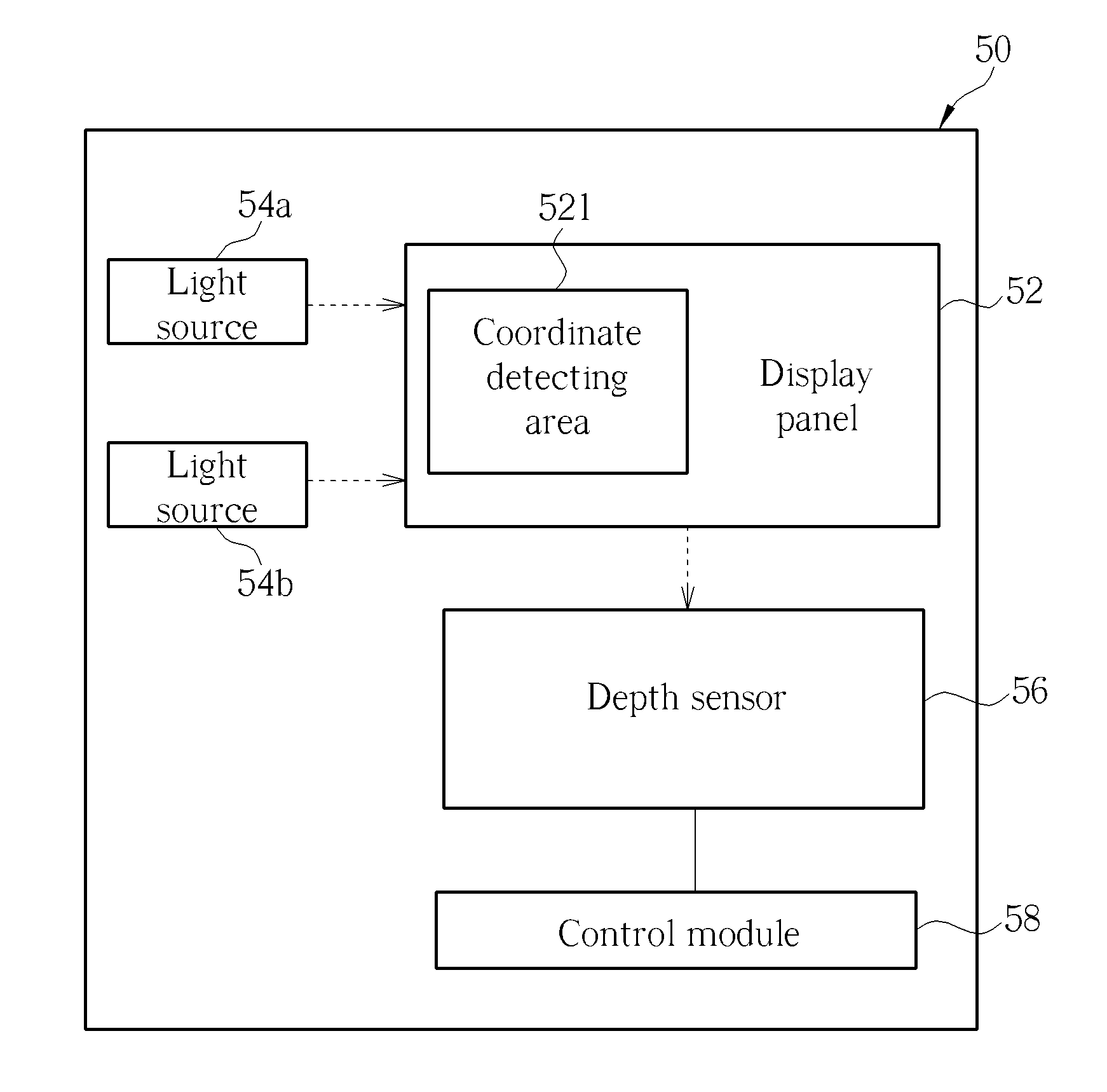
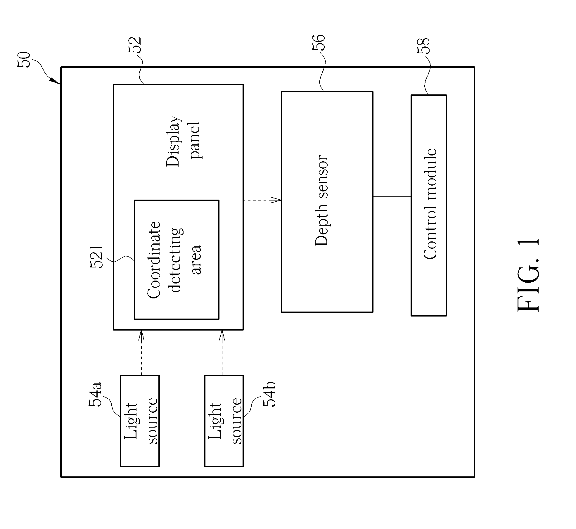
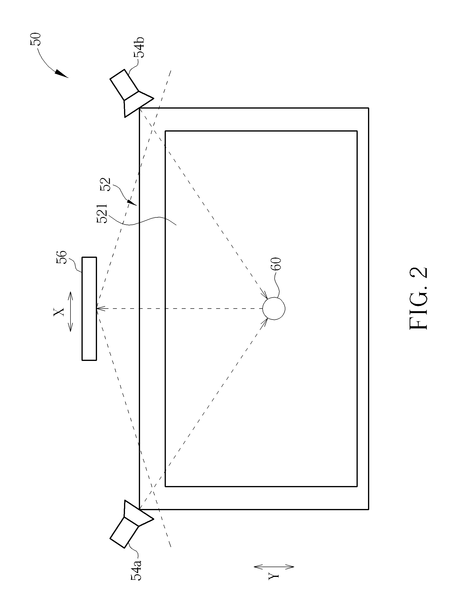
[0023]Please refer to FIG. 1 to FIG. 3. FIG. 1 is a functional block diagram of an optical image device 50 according to an embodiment of the present invention. FIG. 2 and FIG. 3 are respectively a front view and a side view of the optical image device 50 according to the embodiment of the present invention. The optical image device 50 includes a display panel 52, two light sources 54a and 54b, a depth sensor 56 and a control module 58. The display panel 52 can be a touch panel whereon a coordinate detecting area 521 is formed. The two light sources 54a and 54b are respectively disposed at two corners outside the display panel 52, and the two light sources 54a and 54b are used for emitting light to illuminate an object 60. The two light sources 54a and 54b can be a laser light emitting diode or an infrared light emitting diode respectively. Positions and an amount of the light sources are not limited to this embodiment described above, and it depends on actual demand. The depth senso...


PUM


Abstract

An optical imaging device includes a display panel whereon a coordinate detecting area is formed, at least one light source disposed outside the display panel for emitting light to illuminate an object, and a depth sensor installed on a side of the display panel for sensing image data of the object. The image data include a width information corresponding to a distance between the object and the depth sensor in a first direction, and a depth information corresponding to a distance between the object and the depth sensor in a second direction. The optical imaging device further includes a control module coupled to the depth sensor for receiving the image data sensed by the depth sensor and for determining whether to calculate a coordinate value of the object according to the width information and the depth information.

Description

BACKGROUND OF THE INVENTION[0001]1. Field of the Invention[0002]The Present invention relates to an optical imaging device by using a depth sensor and an imaging processing method, and more particularly, to an optical imaging device and an imaging processing method without using a reflecting frame and being capable of forming a detecting area with an unlimited shape.[0003]2. Description of the Prior Art[0004]In the modern consumer electronic products, a portable electronic product such as a personal digital assistant, a smart phone or a mobile phone is equipped with a touch control device as an interface for data transmission. Since consumer electronic products have become lighter, thinner, shorter and smaller, there is no space on these products for containing a conventional input device, such as a mouse, a keyboard and so on. Furthermore, with development of tablet computers focusing on humanity design, a display with the touch control device has gradually become one of the key co...

Claims


Application Information

Patent Timeline
Patent Type & Authority Applications(United States)
IPC IPC(8): H04N5/225
CPCG06F3/042
Inventor CHEN, YU-YENHUANG, PO-LIANG
Owner WISTRON CORP
Why Eureka
Try Eureka