Mounting structure

Active Publication Date: 2013-03-07
MURATA MFG CO LTD
View PDF0 Cites 27 Cited by
  • Summary
  • Abstract
  • Description
  • Claims
  • Application Information

AI Technical Summary

Benefits of technology

[0011]In the mounting structure according to the second preferred embodiment, since the first land portion and the second land portion are not overlapped with the central portion of the first end surface when looking at the laminate in a plan view from the direction normal to the board body and the conductive material is also not overlapped with the central portion of the first end surface when looking at the laminate in a plan view from the direction normal to the board body, the land electrode and the conductive material actin

Problems solved by technology

In an electronic component made up of dielectric layers and capacitor conductors successively laminated (stacked) on each other, when an AC voltage is applied to the electronic component, the applied voltage causes distortions induced by an electric field in the dielectric layers.
Those electric-field induced distortions vibrate a board on which the electronic component is mounted, th

Method used


Image

  • Mounting structure
  • Mounting structure
  • Mounting structure

Examples


first preferred embodiment

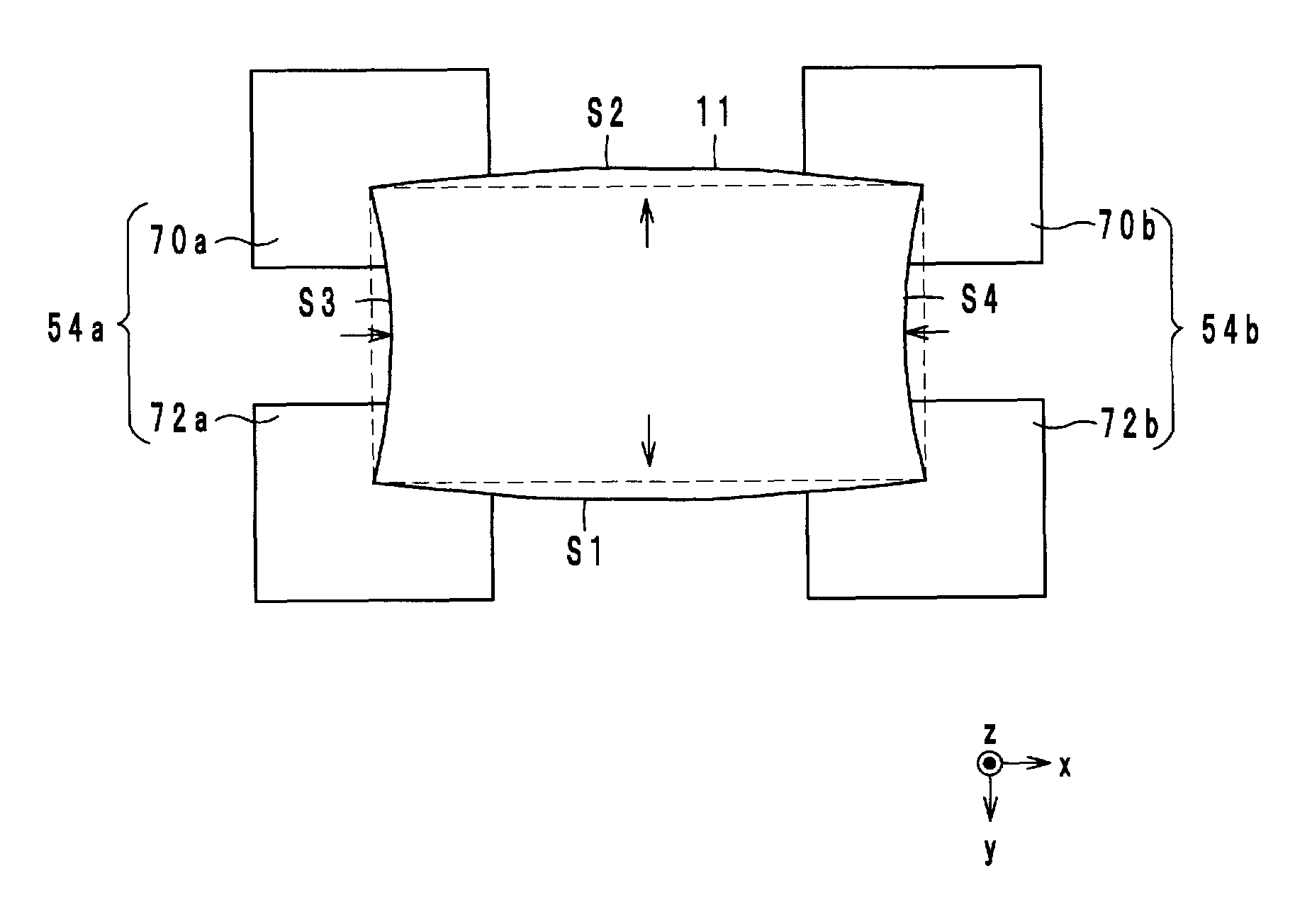
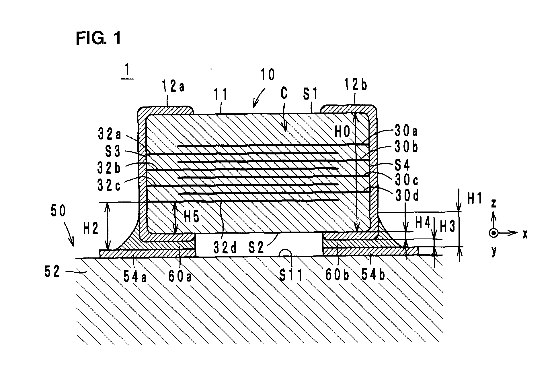
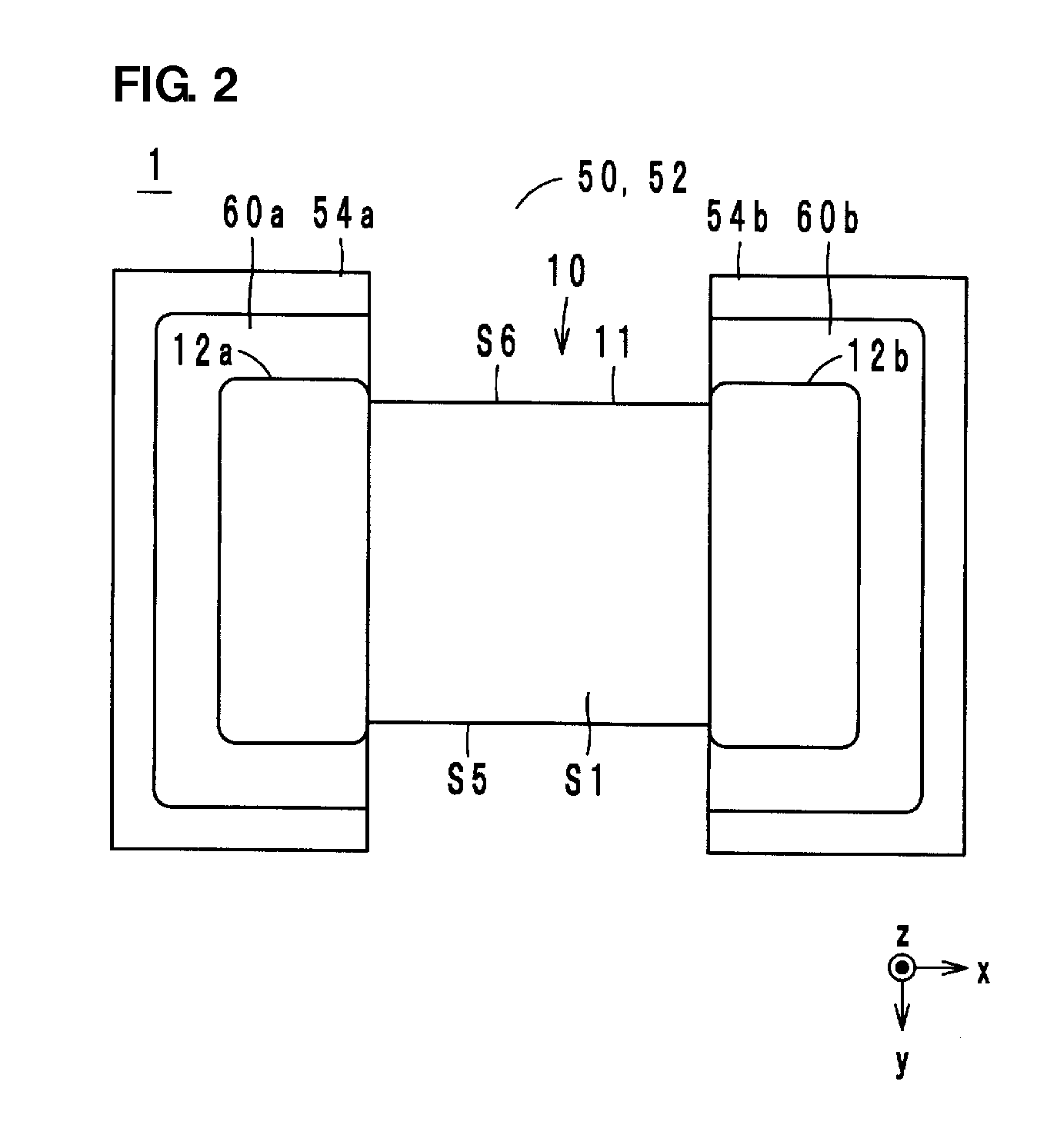
[0030]First, a mounting structure 1 according to a first preferred embodiment is described with reference to FIGS. 1 to 4. As illustrated in FIGS. 1 and 2, the mounting structure 1 includes an electronic component 10 and a circuit board 50. The electronic component 10 preferably is a chip capacitor, for example, and is mounted on the circuit board 50. As also illustrated in FIGS. 3 and 4, the electronic component 10 includes a laminate 11, outer electrodes 12 (12a and 12b), and capacitor conductors 30 (30a to 30d) and 32 (32a to 32d). In the following description, a lamination direction in which multiple layers are laminated in the laminate 11 is defined as a z-axis direction. A direction in which a long side of the laminate 11 extends when looking at the laminate 11 in a plan view from the z-axis direction is defined as an x-axis direction. A direction in which a short side of the laminate 11 extends when looking at the laminate 11 in a plan view from the z-axis direction is define...

second preferred embodiment

[0100]A mounting structure 2 according to a second preferred embodiment will be described below with reference to the drawings. FIG. 12 is a sectional structural view of the mounting structure 2 according to the second preferred embodiment. FIG. 13 is a plan view of the mounting structure 2 illustrated in FIG. 12 when viewed from the positive side in the z-axis direction.

[0101]The mounting structure 2 differs from the above-described mounting structure 1 in the orientation of the electronic component 10. In the mounting structure 2, the lateral surface S5 positioned on one side of the laminate 11 in the direction perpendicular or substantially perpendicular to the lamination direction serves as a mounting surface. In the second preferred embodiment, the lamination direction is defined as the y-axis direction. Further, when looking at the laminate 11 in a plan view from the y-axis direction, a direction in which the long side of the laminate 11 extends is defined as the x-axis direct...


PUM

PropertyMeasurementUnit
Shapeaaaaaaaaaa
Electrical conductoraaaaaaaaaa
Distanceaaaaaaaaaa

Abstract

A mounting structure includes an electronic component mounted on a circuit board. Land electrodes are disposed on a board body and are connected to outer electrodes of the electronic component through solders, respectively. A distance from each of the land electrodes to a top of the corresponding solder is not larger than about 1.27 times a distance from each of the land electrodes to an exposed portion of a capacitor conductor exposed at an end surface of the electronic component, the capacitor conductor being positioned closest to the circuit board.

Description

BACKGROUND OF THE INVENTION[0001]1. Field of the Invention[0002]The present invention relates to a mounting structure, and more particularly to a mounting structure in which an electronic component, such as a capacitor, is mounted on a board.[0003]2. Description of the Related Art[0004]In an electronic component made up of dielectric layers and capacitor conductors successively laminated (stacked) on each other, when an AC voltage is applied to the electronic component, the applied voltage causes distortions induced by an electric field in the dielectric layers. Those electric-field induced distortions vibrate a board on which the electronic component is mounted, thereby generating vibration sounds called “acoustic noise”. As an invention concerning a related-art electronic component intended to reduce the “acoustic noise”, there is known, for example, Japanese Unexamined Patent Application Publication No. 2000-232030 that discloses a circuit board mounting method for a monolithic c...

Claims


Application Information

Patent Timeline
IPC IPC(8): H05K1/16
CPCH05K1/16H05K1/0216H05K2201/2045H05K3/3442H05K1/111Y02P70/50H01G2/06H01G4/12H05K1/18
Inventor FUJII, YASUONISHIOKA, YOSHINAO
Owner MURATA MFG CO LTD
Why Eureka
Try Eureka