Electronic component

Active Publication Date: 2013-03-07
TDK CORPARATION
View PDF3 Cites 27 Cited by
  • Summary
  • Abstract
  • Description
  • Claims
  • Application Information

AI Technical Summary

Benefits of technology

[0008]The inner structure of the electronic component must be changed greatly from that of conventional electronic components. The external electrodes cannot be formed in facilities used for the conventional electronic components. Surfaces at which inner conductors arranged within the electronic component are exposed must be aligned by some techniques before forming the external electrodes. These greatly increase the cost.
[0009]The external electrode has an area much smaller than that of the conventional external electrode having the five-face electrode structure. Therefore, when barrel, plating, which is typically used because of its low cost and favorable productivity, is employed, for forming the plating layer in the external electrode, the probability of energizing a plating cathode through media (metal balls) is low. As a result, the plating takes a long time, e.g., five times or more that of the conventional one, thereby lowering the productivity. The plating has been known to remarkably worsen the reliability of multilayer ceramic capacitors in particular by infiltrating their element bodi

Problems solved by technology

100051 However, the electronic component disclosed in Japanese Patent Application Laid-Open No. 2001-267176 has the following problems.
The external electrodes cannot be formed in facilities used for the conventional electronic components.
These greatly increase the cost.
Therefore, when barrel, plating, which is typically used because of its low cost and favorable productivity, is employed, for forming the plating layer in the external electrode, the probability of energizing a plat

Method used


Image

  • Electronic component
  • Electronic component
  • Electronic component

Examples


Example

[0031]The preferred embodiments of the present invention will be described below in detail with reference to the accompanying drawings. In the description, the same elements or elements with the same functionality will be denoted by the same reference signs, without redundant description.

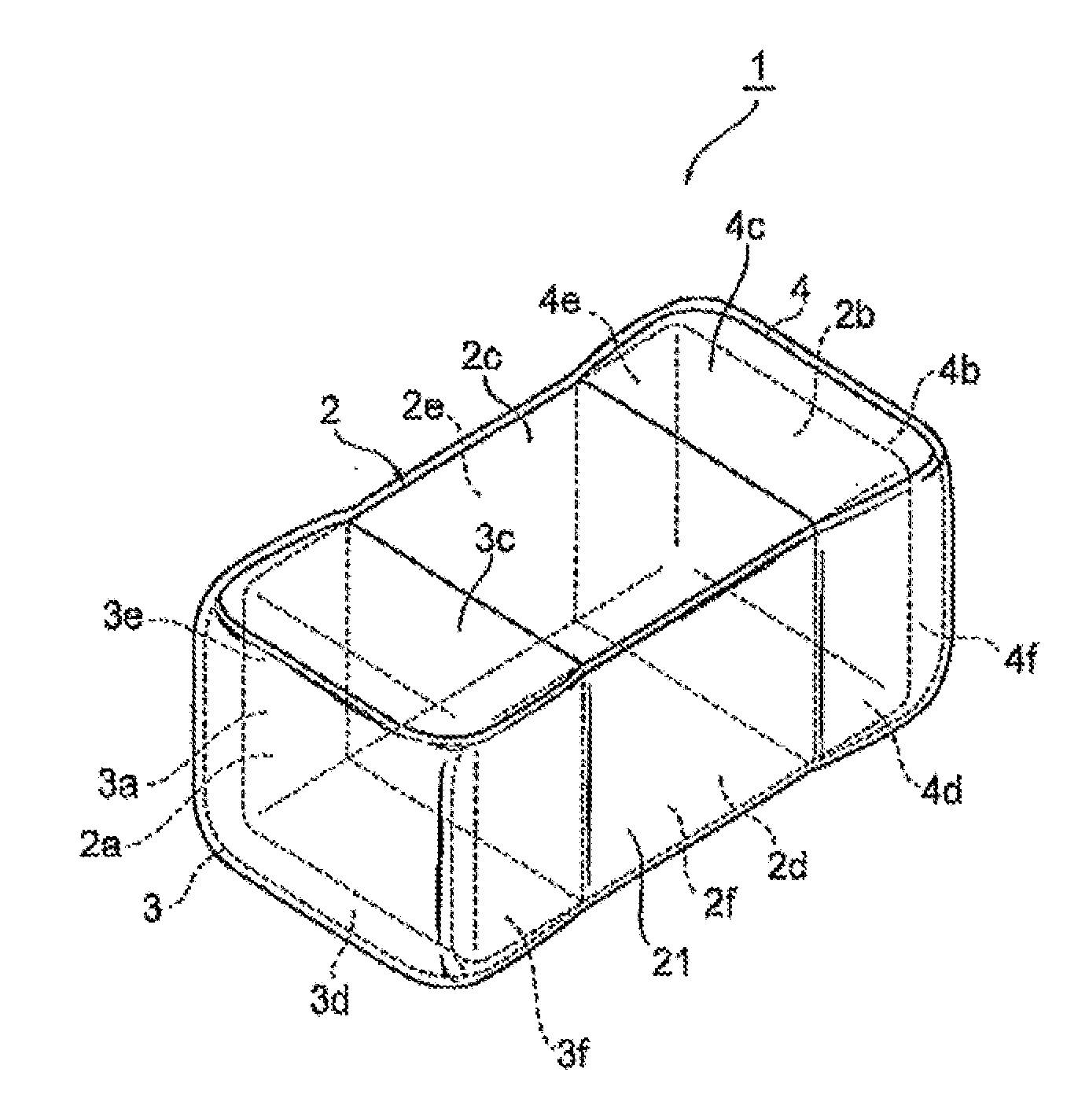
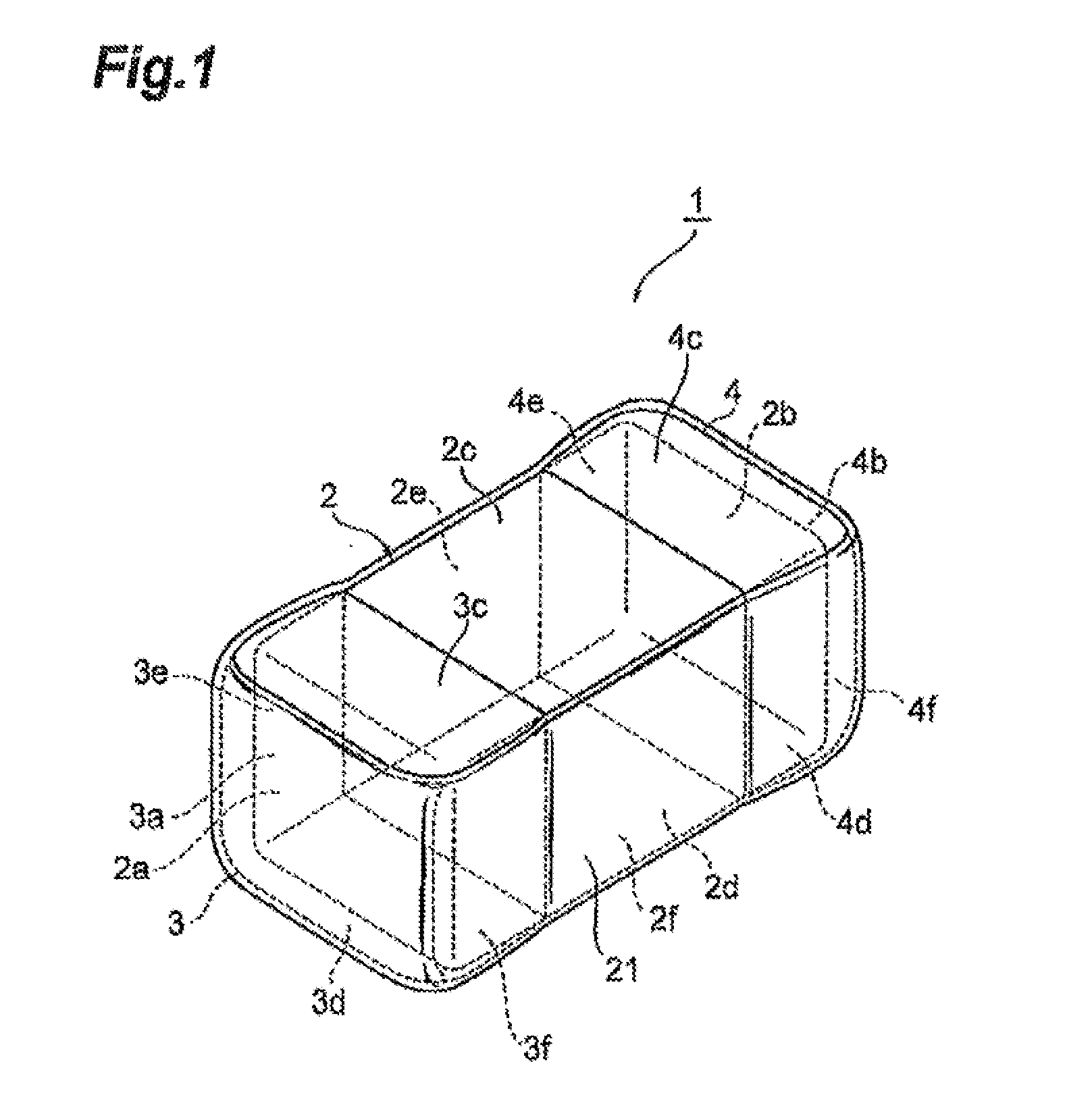
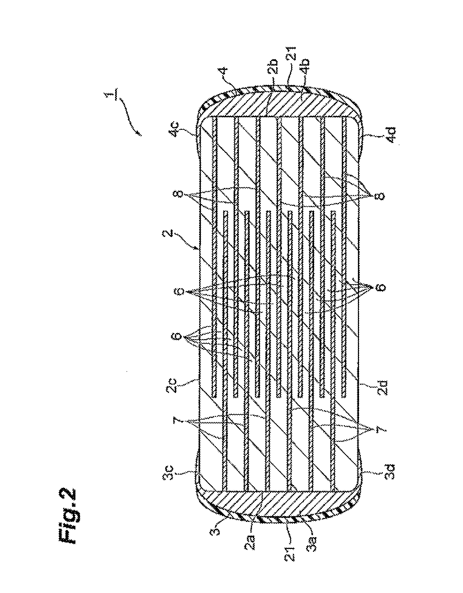
[0032]With reference to FIGS. 1 to 3, configurations of an electronic component 1 in accordance with an embodiment will be explained. FIG. 1 is a perspective view illustrating the electronic component in accordance with the present embodiment. FIGS. 2 and 3 are diagrams for explaining cross-sectional configuration of the electronic component in accordance with the embodiment. FIG. 3 does not depict internal electrodes 7, 8 which will be explained later and the like.

[0033]The electronic component 1, an example of which is a multilayer ceramic capacitor, comprises an element body 2 and a plurality of external electrodes 3, 4. The element body 2 is constructed as a rectangular parallelepiped by stackin...


PUM


Abstract

An electronic component comprises an element body, an external electrode, and an insulating resin coating layer. The element body has a pair of end faces opposed to each other, a pair of principal faces extending so as to connect the pair of end faces and opposed to each other, and a pair of side faces extending so as to connect the pair of principal faces and opposed to each other. The external electrode is formed so as to cover at least a partial region of the principal face and/or a partial region of the side face and has a plating layer comprised of Sn or an Sn alloy. The insulating resin coating layer covers at least the portion of the external electrode formed so as to cover the side face.

Description

BACKGROUND OF THE INVENTION[0001]1. Field of the Invention[0002]the present invention relates to an electronic component,[0003]2. Related Background Art[0004]Known as a surface mounting electronic component (e.g., a multi layer ceramic capacitor) is one comprising an element body having a pair of end faces opposed to each other, a pair of principal faces extending so as to connect the pair of end faces and opposed to each other, and a pair of side faces extending, so as to connect the pair of principal faces and opposed to each other and an external electrode formed so as to cover a partial region of the principal face and / or a partial region of the side face and having a plating layer comprised of Sn or an Sn alloy (see, for example, Japanese Patent Application Laid-Open No. 2006-013315). In the electronic component disclosed in Japanese Patent Application Laid-Open No. 2006-013315, the external electrodes, each having a five-face electrode structure (a structure formed over five s...

Claims


Application Information

Patent Timeline
IPC IPC(8): H05K7/00H01C7/10H01L41/00H01C7/00H01G4/224H01F5/00
CPCH01C1/148H01G4/224H01G4/2325H01G4/232H01G4/12H01G4/30H01G4/248H01G4/228
Inventor SHIRAKAWA, YUKIHIKONAKAMURA, KAZUHIROKON, SHINTARONOGIWA, HIROMITSU
Owner TDK CORPARATION
Why Eureka
Try Eureka