Image sensor and method for fabricating the same

a technology of image sensor and manufacturing method, which is applied in the field of image sensor, can solve the problems of image distortion, correspondingly reduced sensitivity of mos image sensor, and increase and achieve the effect of increasing the processing accuracy of image sensor and increasing the cost of additional costs

Active Publication Date: 2013-03-21
UNITED MICROELECTRONICS CORP
View PDF10 Cites 43 Cited by
  • Summary
  • Abstract
  • Description
  • Claims
  • Application Information

AI Technical Summary

Benefits of technology

[0017]In accordance with the aforementioned embodiments of the present invention, an image sensor and the fabricating method thereof are provided, wherein a plurality of photoelectric transducer devices and an interconnect structure are firstly formed on a front-side surface of a substrate. At least one dielectric isolator extending downwards into the substrate from a back-side surface of the substrate opposite to the back-side surface is then formed in order to isolate the photoelectric transducer devices, whereby both of the incident light passing into the substrate and the photo-carriers generated in the substrate can be effectively isolated. Therefore, the electrical and optical crosstalk between two adjacent photoelectric transducer devices can be avoided.
[0019]Furthermore, since a back-side alignment mark referencing to a front-side alignment mark previously formed on the front-side surface of the substrate for the front-side process can be simultaneous with the formation of the dielectric isolator on the back-side surface by the same steps, thus the subsequent process can be performed more precisely without performing any additional process. In other words, the processing accuracy of the image sensor can be significantly increased without increasing any additional cost.

Problems solved by technology

However, reduction in the physical size and pixel pitch of the photoelectric transducer devices may result in electrical and optical crosstalk between two adjacent photoelectric transducer devices, the sensitivity of the MOS image sensor is thus correspondingly reduced and, in the worst case, image distortion may occur.
However, the STI which has limited depth may not possible to satisfactorily provide an electrical crosstalk barrier.
Furthermore, the STI does not provide an effective optical crosstalk barrier when a backside image sensor is fabricated.

Method used


Image

  • Image sensor and method for fabricating the same
  • Image sensor and method for fabricating the same
  • Image sensor and method for fabricating the same

Examples


Embodiment Construction

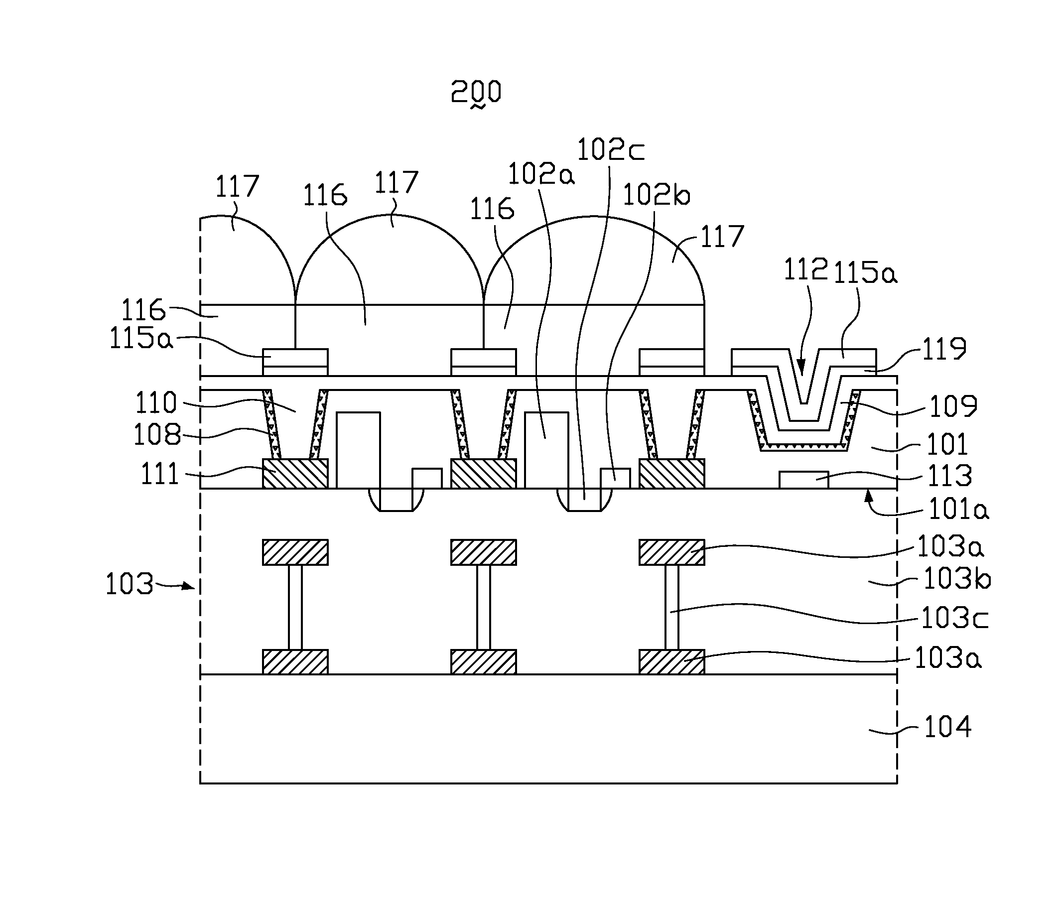
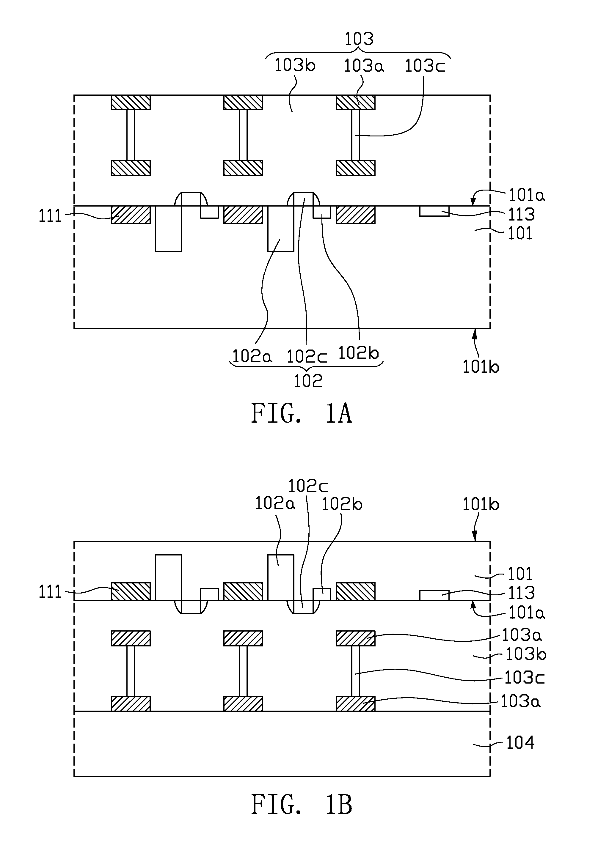
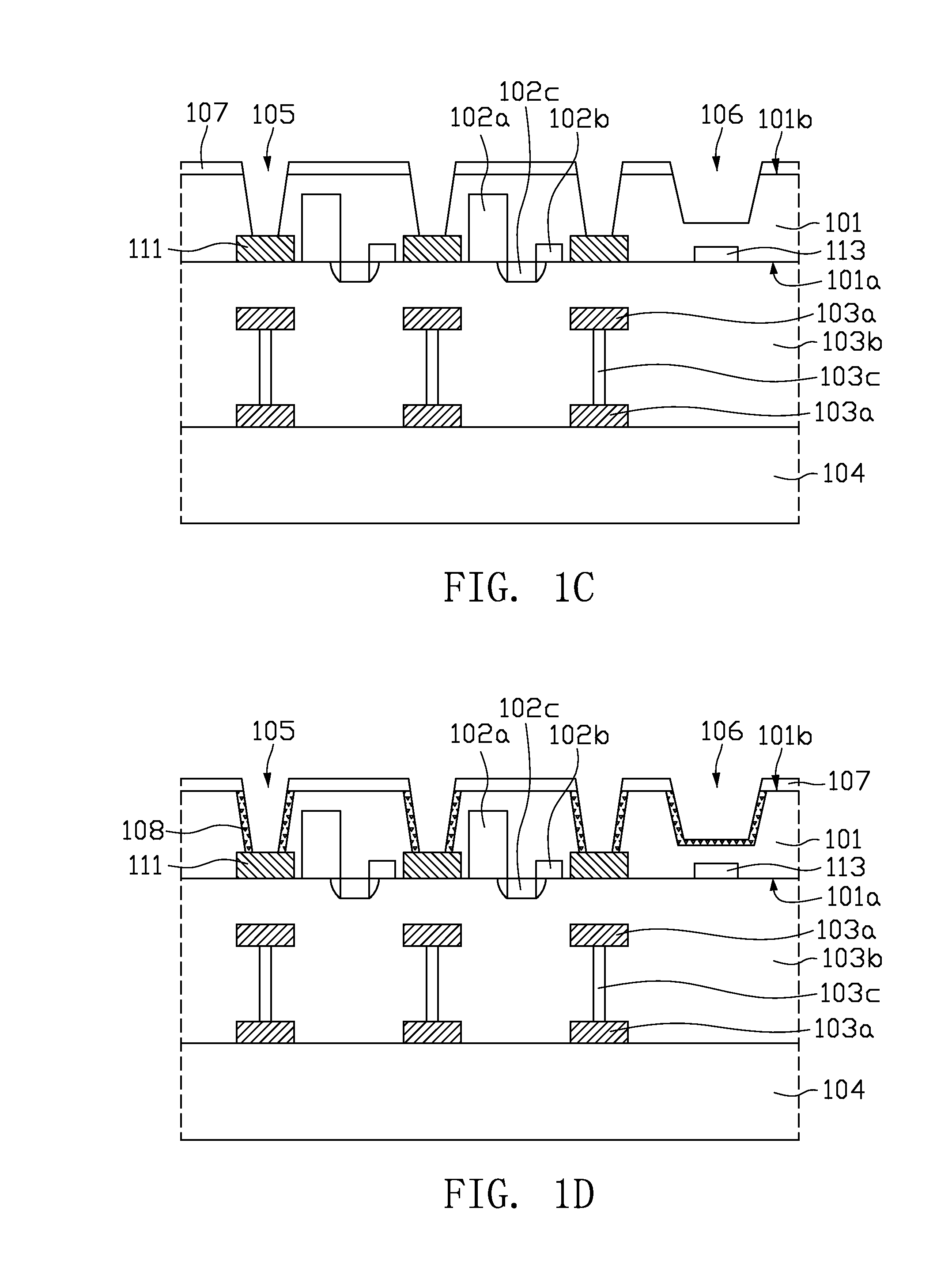
[0023]The present invention is to provide an image sensor and the method for fabricating the same to avoid the problems of electrical and optical crosstalk, meanwhile, the processing accuracy of the image sensor can be significantly increased. The present invention will now be described more specifically with reference to the following embodiment for fabricating a MOS image sensor 100. It is to be noted that the following descriptions of preferred embodiments of this invention are presented herein for purpose of illustration and description only. It is not intended to be exhaustive or to be limited to the precise form disclosed.

[0024]FIGS. 1A to 1J are cross sectional views illustrating a method for fabricating a MOS image sensor 100 in accordance with one embodiment of the present invention. As shown in FIG. 1A, a substrate 101 having a front-side surface 101a and a back-side surface 101b opposite to the front-side surface 101a is firstly provided. A front-side process is then perf...


PUM


Abstract

An image sensor comprises a substrate, a plurality of photoelectric transducer devices, an interconnect structure, at least one dielectric isolator and a back-side alignment mark. The substrate has a front-side surface and a back-side surface opposite to the front-side surface. The interconnect structure is disposed on the front-side surface. The photoelectric transducer devices are formed on the front-side surface. The dielectric isolator extends downwards into the substrate from the back-side surface in order to isolate the photoelectric transducer devices. The back-side alignment mark extends downwards into the substrate from the back-side surface and references to a front-side alignment mark previously formed on the front-side surface.

Description

FIELD OF THE INVENTION[0001]The present invention relates to a semiconductor device and the method for fabricating the same, more particularly to an image sensor and the method for fabricating the same.BACKGROUND OF THE INVENTION[0002]An image sensor, such as a metal-oxide-semiconductor (MOS) image sensor is a photoelectric device which can convert optical images into electrical signals and has been widely applied in various consumer products such as, digital cameras, camcorders, personal communication systems (PCSs), game equipment, requiring for improved image resolution.[0003]In order to satisfy the demands for finer image resolution capabilities, it is necessary to increase the pixel integration of MOS image sensors, and the size and pixel pitch of the constituent photoelectric transducer device, (e.g., a photodiode) shall be shrank. However, reduction in the physical size and pixel pitch of the photoelectric transducer devices may result in electrical and optical crosstalk betw...

Claims


Application Information

Patent Timeline
Patent Type & Authority Applications(United States)
IPC IPC(8): H01L31/0232H01L31/18
CPCH01L27/1463H01L27/14636H01L27/14689H01L27/14687H01L27/1464
Inventor KAO, CHING-HUNGWU, HSIN-PING
Owner UNITED MICROELECTRONICS CORP
Why Eureka
Try Eureka