Semiconductor device operates on external and internal power supply voltages and data processing system including the same

a technology of magnetic field and power supply voltage, applied in the field of magnetic field, can solve the problems of inability to shorten the time from issuing a read command to outputting first data

Active Publication Date: 2013-03-21
LONGITUDE LICENSING LTD
View PDF5 Cites 4 Cited by
  • Summary
  • Abstract
  • Description
  • Claims
  • Application Information

AI Technical Summary

Benefits of technology

[0018]In an aspect of this disclosure, there is provided a device comprising: an output terminal; and an output unit coupled to the output terminal, the output unit comprising; an output buffer coupled to the output terminal and operating on a first power supply voltage, a first control circuit operating on a second power supply voltage, receiving an impedance adjustment signal and a data signal and making the output buffer drive the output terminal to a first logic level designated by the data signal with impedance designated by the impedance adjustment signal, the second power supply voltage being smaller in level than the first power supply voltage; and a level shifter coupled between the output buffer and the first control circuit, the level shifter including a first circuit portion operating on the second power supply voltage and a second circuit portion operating on the first power supply voltage.
[0019]Another aspect of the disclosure, there is provided an output terminal, an output buffer including a power supply node supplied with a first power supply voltage and a plurality of transistors coupled in parallel between the power supply node and the output terminal; a first control circuit operating on a second power supply voltage, receiving an impedance adjustment signal and a data signal and making one or ones of the transistors, that designated by the impedance adjustment signal, conductive to drive the output terminal to a first logic level designated by the data signal, the second power supply voltage being smaller in level than the first power supply voltage; and a plurality of level shift circuits each coupled between the first control circuit and a control electrode of an associated one of the transistors, each of the level shift circuits including a first circuit portion operating on the second power supply voltage and a second circuit portion operating on the first power supply voltage.

Problems solved by technology

However, because a DRAM core is consistently operated by an analog operation also in the synchronous DRAM, a considerably weak charge needs to be amplified by a sensing operation.
Accordingly, it is not possible to shorten the time from issuing a read command to outputting first data.
However, when the internal voltage is used in a semiconductor device that uses a latency counter, there is a possibility that the margin (or latch margin of the latency counter) decreases at a time when the internal read command MDRDT is accepted in synchronism with the input gate signal CIT, and the process of accepting the internal read command MDRDT could fail as a result.
As a result, a difference in phase occurs between the internal read command MDRDT and the input gate signal CIT, leading to a decline in the latch margin of the latency counter.
In some cases, the process of accepting the internal read command MDRDT could fail.

Method used


Image

  • Semiconductor device operates on external and internal power supply voltages and data processing system including the same
  • Semiconductor device operates on external and internal power supply voltages and data processing system including the same
  • Semiconductor device operates on external and internal power supply voltages and data processing system including the same

Examples


Embodiment Construction

[0036]Preferred embodiments of the present invention will be explained below in detail with reference to the accompanying drawings.

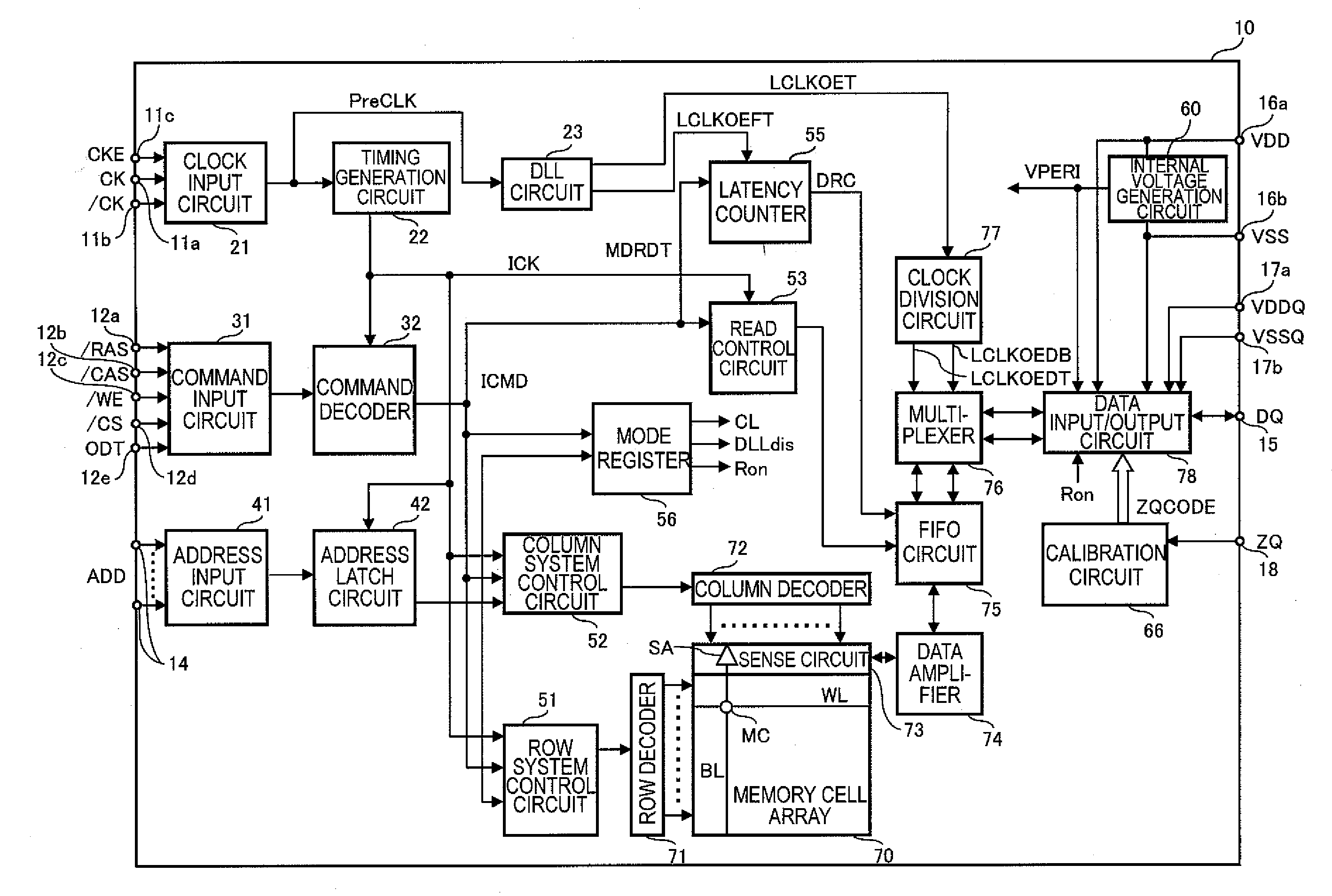
[0037]Referring now to FIG. 1, the semiconductor device 10 of the present embodiment is a synchronous DRAM, and includes the following external terminals: clock terminals 11a and 11b; a clock enable terminal 11c; command terminals 12a to 12e; address terminals 14; a data input / output terminal 15; power supply terminals 16a, 16b, 17a, and 17b; and a calibration terminal 18.

[0038]The clock terminals 11a and 11b are terminals to which external clock signals CK and / CK are respectively supplied. The clock enable terminal 11c is a terminal to which a clock enable signal CKE is input. The supplied external clock signals CK and / CK and clock enable signal CKE are supplied to a clock input circuit 21. In the present specification, a signal whose name starts with “ / ” means an inverted signal of a corresponding signal, or a low-active signal. Accordingly, the cloc...


PUM


Abstract

The semiconductor device including an output terminal; and an output unit coupled to the output terminal. The output unit includes an output buffer coupled to the output terminal and operating on a first power supply voltage, a first control circuit operating on a second power supply voltage, receiving an impedance adjustment signal and a data signal and making the output buffer drive the output terminal to a first logic level designated by the data signal with impedance designated by the impedance adjustment signal, and a level shifter coupled between the output buffer and the first control circuit. The second power supply voltage is smaller in level than the first power supply voltage. The level shifter includes a first circuit portion operating on the second power supply voltage and a second circuit portion operating on the first power supply voltage.

Description

BACKGROUND OF THE INVENTION[0001]1. Field of the Invention[0002]The present invention relates to a semiconductor device, and particularly to a semiconductor device that controls output timing of data using a latency counter. The present invention also relates to a data processing system including such a semiconductor device.[0003]2. Description of Related Art[0004]Synchronous memory devices represented by a synchronous DRAM (Synchronous Dynamic Random Access Memory) are widely used as a main memory or the like of personal computers. In the synchronous memory device, data is inputted and outputted in synchronism with a clock signal supplied from a controller. Thus, when a higher-speed clock signal is used, the data transfer rate can be increased.[0005]However, because a DRAM core is consistently operated by an analog operation also in the synchronous DRAM, a considerably weak charge needs to be amplified by a sensing operation. Accordingly, it is not possible to shorten the time from...

Claims


Application Information

Patent Timeline
Patent Type & Authority Applications(United States)
IPC IPC(8): G11C7/10
CPCG11C7/1057
Inventor SATO, TAKENORI
Owner LONGITUDE LICENSING LTD
Why Eureka
Try Eureka