Heating systems for thin film formation
- Summary
- Abstract
- Description
- Claims
- Application Information
AI Technical Summary
Benefits of technology
Problems solved by technology
Method used
Image

Examples
Embodiment Construction
[0029]The present invention is directed to systems of material fabrication. More particularly, the invention provides a heating system for forming epitaxial layers of semiconductor materials. Merely by way of example, the invention has been applied to metal-organic chemical vapor deposition. But it would be recognized that the invention has a much broader range of applicability.
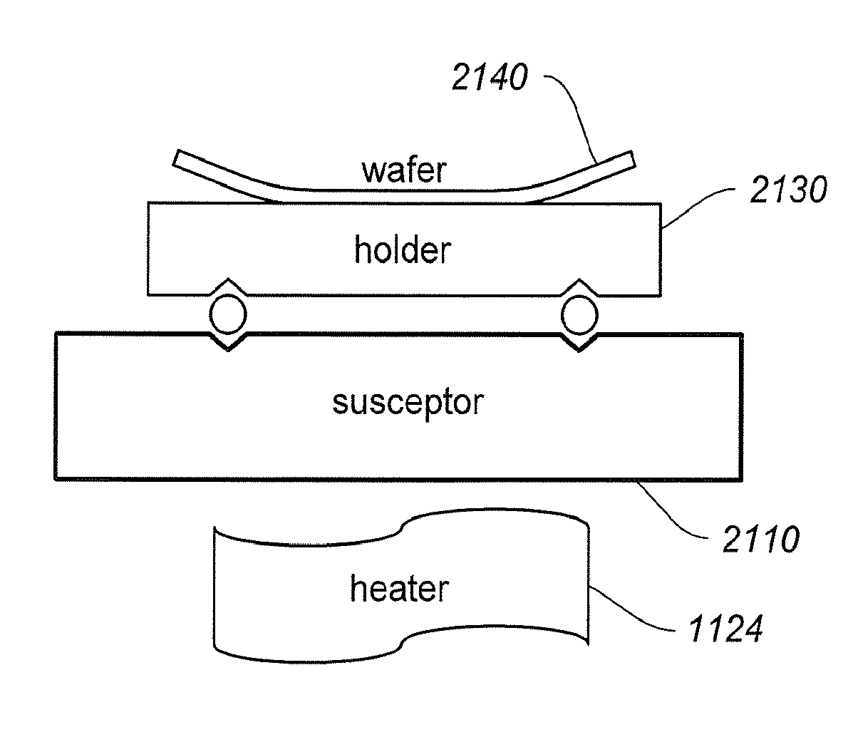
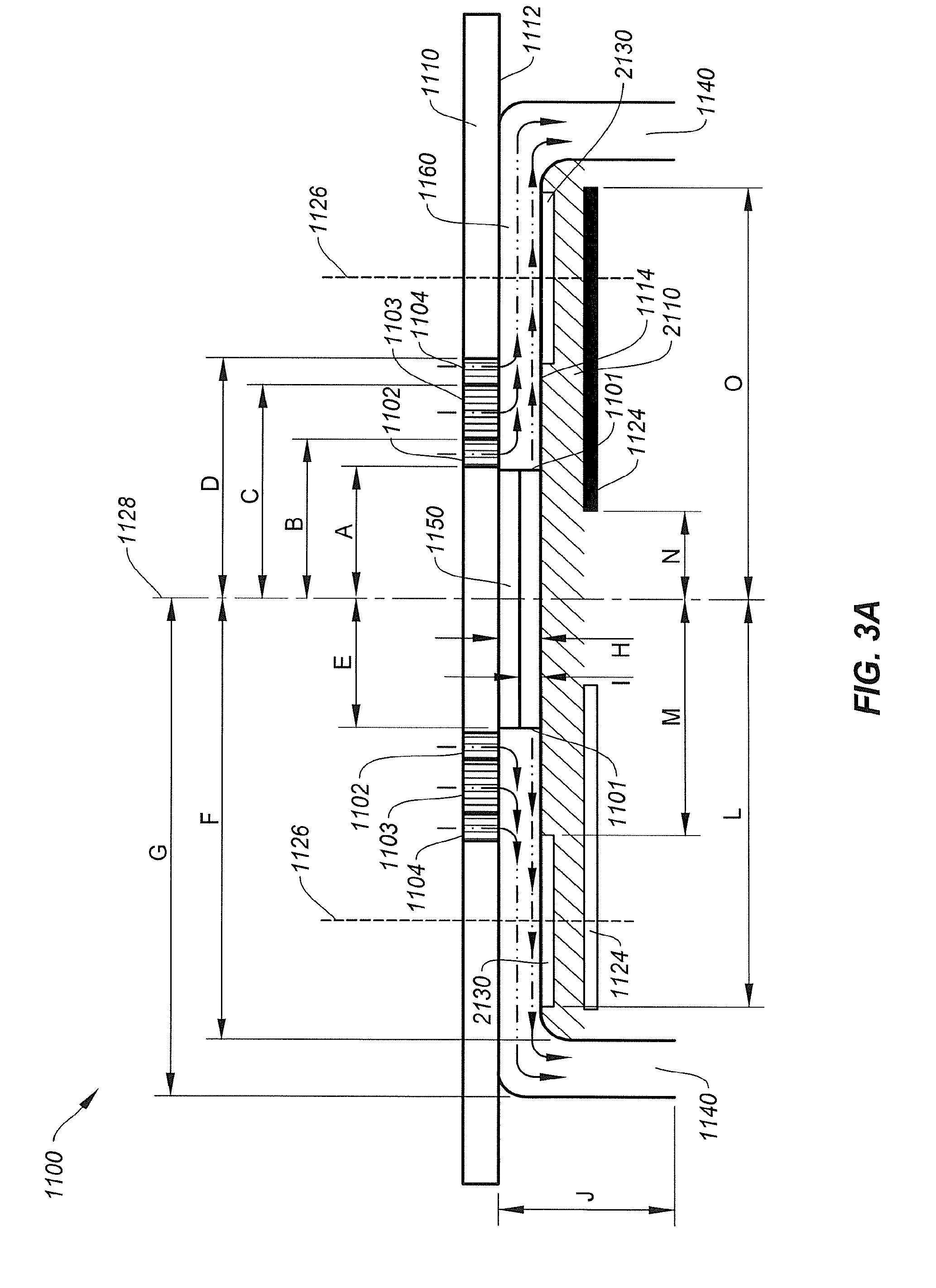
[0030]FIGS. 3(A) and (B) are simplified diagrams showing a reaction system that includes a rotation system for forming one or more materials on one or more substrates according to one embodiment. For example, FIG. 3(A) shows a side view of the reaction system 1100, and FIG. 3(B) shows a planar view of the reaction system 1100. In another example, the reaction system 1100 includes a showerhead component 1110, the susceptor 2110, inlets 1101, 1102, 1103 and 1104, one or more substrate holders 2130, one or more heating devices 1124, an outlet 1140, and a central component 1150. In yet another example, the centra...
PUM
| Property | Measurement | Unit |
|---|---|---|
| Temperature | aaaaa | aaaaa |
| Dimension | aaaaa | aaaaa |
| Transparency | aaaaa | aaaaa |
Abstract
Description
Claims
Application Information