Semiconductor chip, semiconductor device, and method of measuring the same

a semiconductor and chip technology, applied in the field of semiconductor devices, semiconductor devices, and methods of measuring the same, can solve the problems of large amount of man-hours required for continuity tests, large extension of connection failure, and large amount of defective products

Active Publication Date: 2013-03-28
LONGITUDE LICENSING LTD
View PDF6 Cites 29 Cited by
  • Summary
  • Abstract
  • Description
  • Claims
  • Application Information

AI Technical Summary

Problems solved by technology

However, since a great number of TSVs are provided in such a semiconductor device, a huge amount of man-hours are required for continuity tests if a continuity test is performed for every one of the TSVs.
In a case where a continuity test of a TSV is usually carried out after a semiconductor device has been assembled into a product, the entire product becomes defective if any defect is found between TSVs after the assembly.
According to inventors' study, it has been found that, if a connection failure or defect occurs between semiconductor chips, the connection failure widely extends not only to signal through electrodes, but also to the vicinity of the signal through electrodes.

Method used


Image

  • Semiconductor chip, semiconductor device, and method of measuring the same
  • Semiconductor chip, semiconductor device, and method of measuring the same
  • Semiconductor chip, semiconductor device, and method of measuring the same

Examples


Embodiment Construction

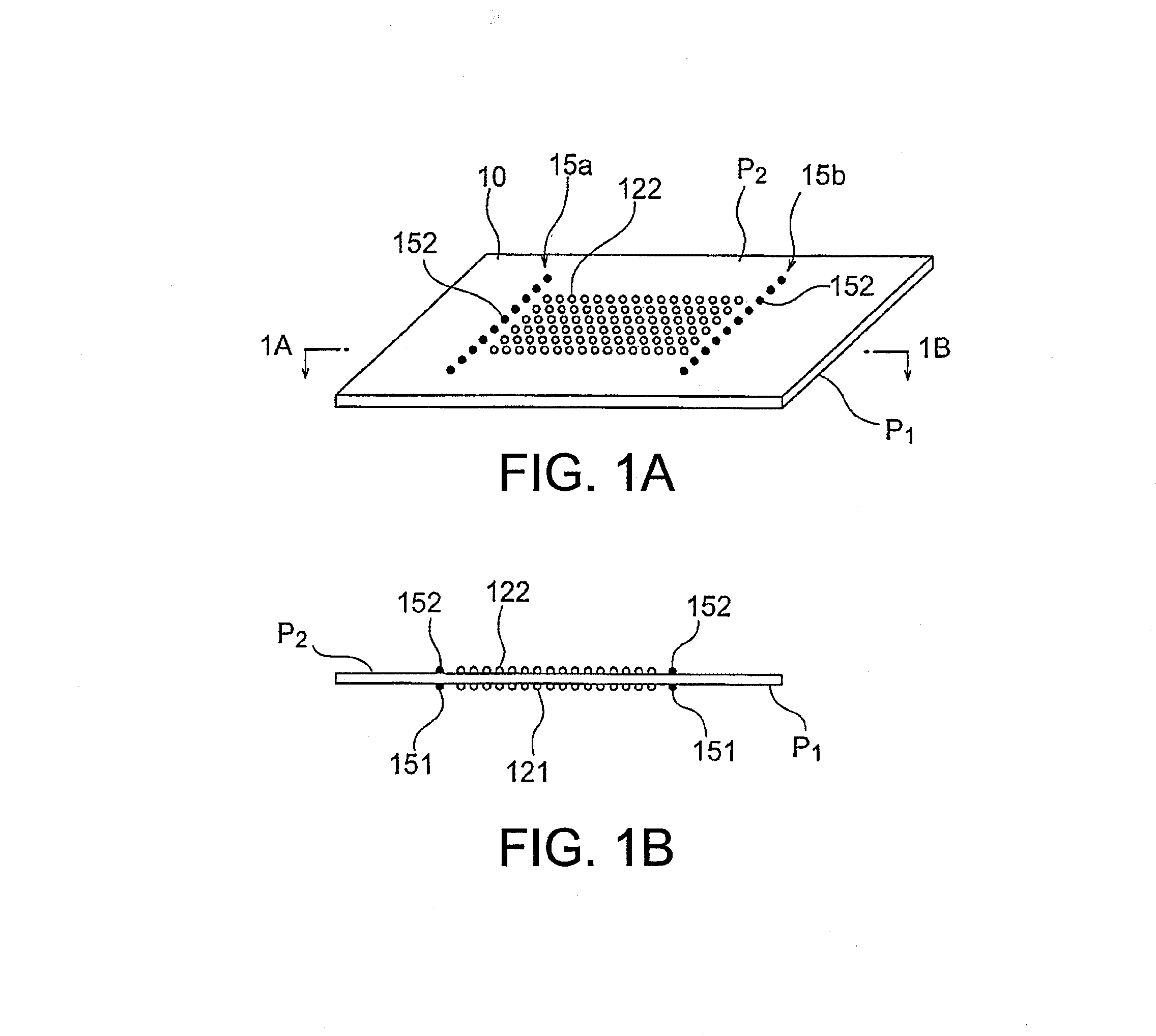
[0035]FIGS. 1A and 1B are a perspective view and a cross-sectional view showing a semiconductor chip 10 according to an embodiment of the present invention. The semiconductor chip 10 will be explained as being a DRAM. Nevertheless, semiconductor chips to which the present invention is applicable are not limited to a DRAM, and the present invention may be applied to an SRAM and a non-volatile memory, such as a flash memory, a ReRAM, an MRAM, a PRAM, and the like. For convenience of explanation, a lower surface of the semiconductor chip 10 illustrated in FIGS. 1A and 1B is referred to as a first surface P1, and an upper surface of the semiconductor chip 10 illustrated in FIGS. 1A and 1B is referred to as a second surface P2.

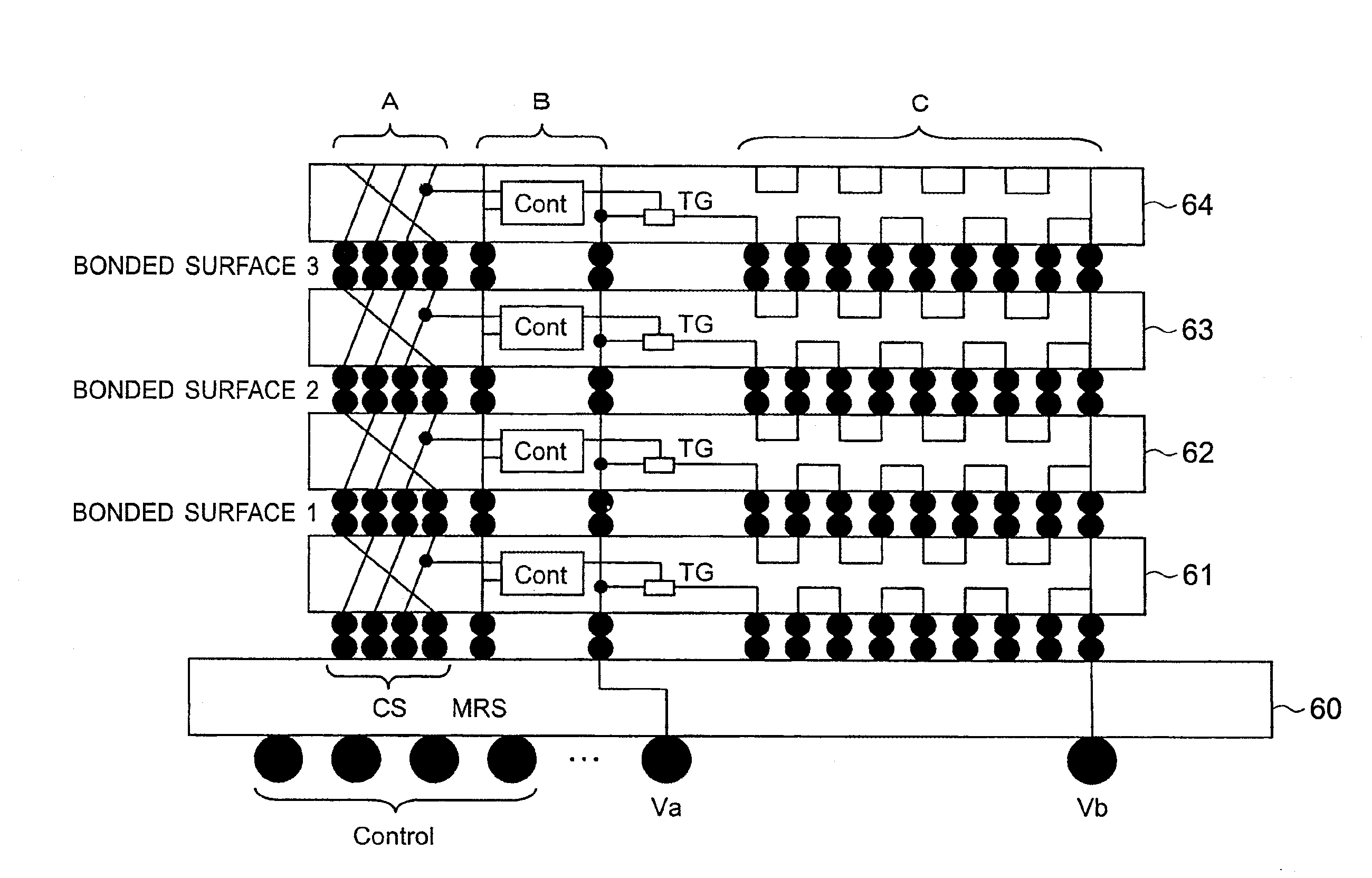
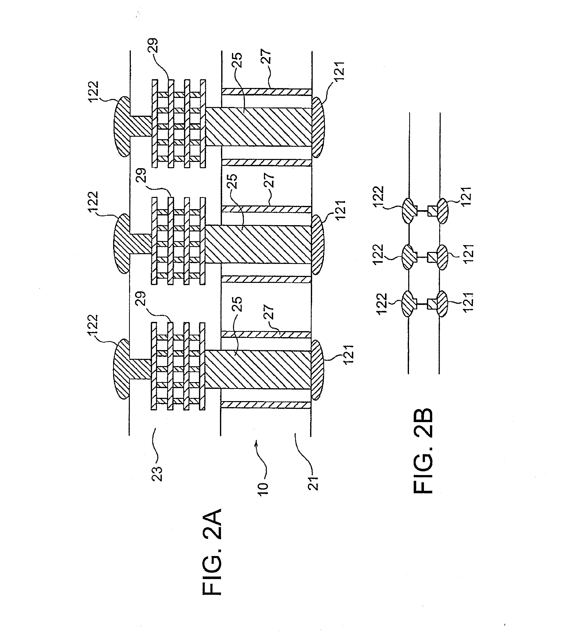
[0036]The semiconductor chip 10 includes a large number of signal through electrodes formed at a central portion of the semiconductor chip 10. Those signal through electrodes are hereinafter referred to as signal TSVs. The signal TSVs extend through the semiconduct...


PUM


Abstract

In a semiconductor device in which semiconductor chips having a number of signal TSVs are stacked, a huge amount of man-hours have been required to perform a continuity test for each of the signal TSVs. According to the present invention, no continuity test is performed directly on signal TSVs. Dummy bumps are arranged in addition to signal TSVs. The dummy bumps of the semiconductor chips are connected through a conduction path that can pass the dummy bumps between the semiconductor chips with one stroke when the semiconductor chips are stacked. A continuity test of the conduction path allows a bonding defect on bonded surfaces of two of the stacked semiconductor chips to be measured and detected.

Description

[0001]This application is based upon and claims the benefit of priority from Japanese patent application No. 2011-210987, filed on Sep. 27, 2011 and Japanese patent application No. 2011-273703, filed on Dec. 14, 2011, the disclosures of which are incorporated herein in their entirety by reference.BACKGROUND[0002]The present invention relates to a semiconductor chip, a semiconductor device having a structure in which semiconductor chips are stacked, and a method of measuring a semiconductor device.[0003]Recently, proposals have been made about a semiconductor device which has a multilayer structure of stacking semiconductor chips through a number of through electrodes, which are called through silicon vias (TSVs). In a semiconductor device having such a multilayer structure, a continuity test or conduction test is performed for each of TSVs after the stacking of semiconductor chips in order to determine whether or not a normal connection is established between the semiconductor chips...

Claims


Application Information

Patent Timeline
Patent Type & Authority Applications(United States)
IPC IPC(8): H01L23/48G01R31/26
CPCG11C29/025H01L25/0657H01L2224/16H01L2924/13091H01L2924/00H01L2225/06506H01L2225/06513
Inventor ISHIKAWA, TORUSEGAWA, MACHIO
Owner LONGITUDE LICENSING LTD
Why Eureka
Try Eureka