
Light-emitting device

Active Publication Date: 2013-04-04
EPISTAR CORP
View PDF4 Cites 11 Cited by
  • Summary
  • Abstract
  • Description
  • Claims
  • Application Information

AI Technical Summary

Benefits of technology

This patent describes a light-emitting device that includes three layers of different energy gaps and thicknesses. These layers are arranged in a specific way to optimize the device's performance. The device produces light when an electric current passes through it. The technical effect of this invention is to provide a more efficient and effective light-emitting device.

Problems solved by technology

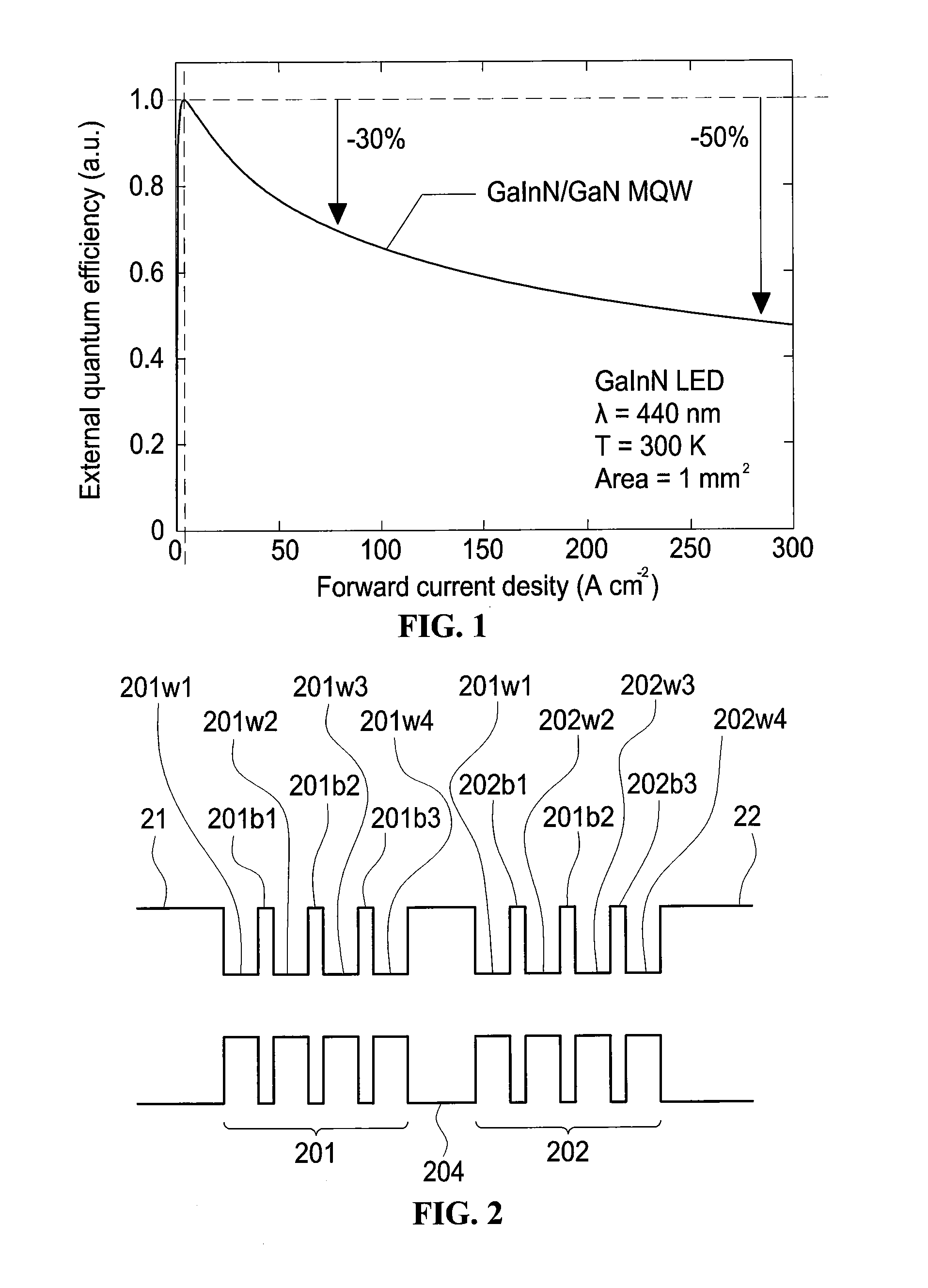
For a conventional light-emitting diode (LED) structure, the device efficiency rises as the operating current increases, but when the operating current increases and reaches a certain value, the device efficiency declines.
This efficiency droop phenomenon limits the efficiency of the LED under a large current.
The cause of this efficiency droop phenomenon is still inconclusive, but it is generally believed that it is due to the mismatch of mobility of the electrons and holes in a high-current operation, so the electrons in the multi-quantum well (MQW) of the light-emitting layer overflows easily to the p-type semiconductor layer, and electrons are unevenly distributed in the multi-quantum well.
Most of the electrons are concentrated in one or several quantum wells near the p-type semiconductor layer, so the holes that are injected into the light-emitting layer are insufficient, and the device efficiency declines in a high-current operation.

Method used


Image

  • Light-emitting device
  • Light-emitting device
  • Light-emitting device

Examples


Embodiment Construction

[0021]FIG. 2 shows the schematic diagram of the energy band gap of a composite super-lattice structure light-emitting layer in accordance with the first embodiment of the present application. The schematic diagram of the energy band gap in this embodiment shows a composite super-lattice structure light-emitting layer comprising a first super-lattice structure light-emitting layer group 201, a second super-lattice structure light-emitting layer group 202, and a spacer barrier layer 204 disposed between the two super-lattice structure light-emitting layer groups 201, 202. The composite super-lattice structure light-emitting layer may be disposed between a first conductivity type semiconductor layer 21 and a second conductivity type semiconductor layer 22 to form a light-emitting device. The first conductivity type semiconductor layer 21 and the second conductivity type semiconductor layer 22 have different conductivity type, for example, the first conductivity type semiconductor layer...


PUM


Abstract

Disclosed is a light-emitting device, comprising: a first multi-quantum well structure comprising a plurality of first well layers and a first barrier layer stacked alternately, wherein the energy gap of the first barrier layer is larger than that of any one of the first well layers; a second multi-quantum well structure comprising a plurality of second well layers and a second barrier layer stacked alternately, wherein the energy gap of the second barrier layer is larger than that of any one of the second well layers; and a third barrier layer disposed between the first multi-quantum well structure and the second multi-quantum well structure, and the third barrier layer connected with the first well layer and the second well layer, wherein the energy gap of the third barrier layer is larger than that of any one of the first well layers and the second well layers, and the thickness of the third barrier layer is larger than that of any one of the first barrier layer and the second barrier layer.

Description

TECHNICAL FIELD[0001]The application relates to a light-emitting device, and more particular to a light-emitting device with an improved luminous efficiency.CROSS REFERENCE TO RELATED APPLICATION[0002]This application claims priority to Taiwan Patent Document No. 100135444, filed on Sep. 29, 2011 with the Taiwan Patent Office, which disclosure is hereby incorporated by reference in its entirety and made a part of this specification.DESCRIPTION OF BACKGROUND ART[0003]For a conventional light-emitting diode (LED) structure, the device efficiency rises as the operating current increases, but when the operating current increases and reaches a certain value, the device efficiency declines. Such efficiency declination phenomenon is called “efficiency droop”. As shown in FIG. 1, the external quantum efficiency of the LED device reaches the highest point at a current density of about 10 A / cm2, and when the current density increases, the external quantum efficiency of the device declines dra...

Claims


Application Information

Patent Timeline
IPC IPC(8): H01L33/06H01L33/08
CPCH01L33/06H01L33/32H01L33/08
Inventor HSIEH, MIN-HSUNCHANG, SHIH-PANGYANG, HUNG-CHIHHSU, TA-CHENG
Owner EPISTAR CORP
Learn More