Deposition apparatus and deposition method

Inactive Publication Date: 2002-10-03
SEMICON ENERGY LAB CO LTD
View PDF76 Cites 169 Cited by
  • Summary
  • Abstract
  • Description
  • Claims
  • Application Information

AI Technical Summary

Problems solved by technology

Further, since the organic luminescent element is a carrier-filling type luminescent element, it can be driven by DC voltage, and is hard to generate noise.
That is, in order to have the single-layered organic luminescent element efficiently emitting light (or driving at low voltage), it is necessary to use a material (referred below to as "bipolar material") capable of carrying both electrons and holes in well-balanced manner, and Alq.sub.3 does not meet such requirement.
However, being a junction between substances of different kinds (in particular, a junction between insulating materials), the laminated structure described above will necessarily produce an energy barrier at an interface the substances.
Since the presence of an energy barrier inhibits movements of a carrier at the interface, the two following problems are caused.
One of the problems is that it results in a barrier leading to further reducti

Method used


Image

  • Deposition apparatus and deposition method
  • Deposition apparatus and deposition method
  • Deposition apparatus and deposition method

Examples


embodiment 1

[0104] [Embodiment 1]

[0105] An explanation will be given of the case where the deposition apparatus of the present invention is the inline scheme, with reference to FIG. 5. In FIG. 5. reference numeral 501 denotes a load chamber, from which a substrate is transported. Note that the term substrate as used in this embodiment is to be understood to mean the one with either an anode or cathode (anode used in this embodiment) for use as one electrode of a luminescent element being formed thereon. In addition the load chamber 501 comes with a gas exhaust system 500a, wherein this exhaust system 500a is constituted including a first valve 51, a turbo molecular pump 52, a second valve 53, a third valve 54 and a dry pump 55.

[0106] Additionally in this embodiment, as the material used for inside of respective processing chambers such as a gate-blocked load chamber, an alignment chamber, a deposition chamber, a sealing chamber and an unloading chamber, a material such as aluminum or stainless ...

embodiment 2

[0147] [Embodiment 2]

[0148] A deposition apparatus of the present invention will be explained with reference to FIGS. 7A and 7B. In FIGS. 7A and 7B, reference numeral 701 denotes a transfer chamber, wherein this transfer chamber 701 comprises a transfer mechanism A702 for performing transport of a substrate 703. The transfer chamber 701 is set in a pressure-reduced atmosphere and is coupled by a gate with each processing chamber. A substrate is transported to each processing chamber by the transfer mechanism A702 upon opening of the gate. Additionally while exhaust pump such as a dry pump, a mechanical booster pump, a turbo molecular pump (magnetic floatation type) or cryopump is employable for pressure reduction of the transfer chamber 701, the turbo molecular pump of the magnetic flotation type is preferable in order to obtain high-degree vacuum states with higher purity.

[0149] An explanation will be given of each processing chamber below. Note that the transfer chamber 701 is set...

embodiment 3

[0196] [Embodiment 3]

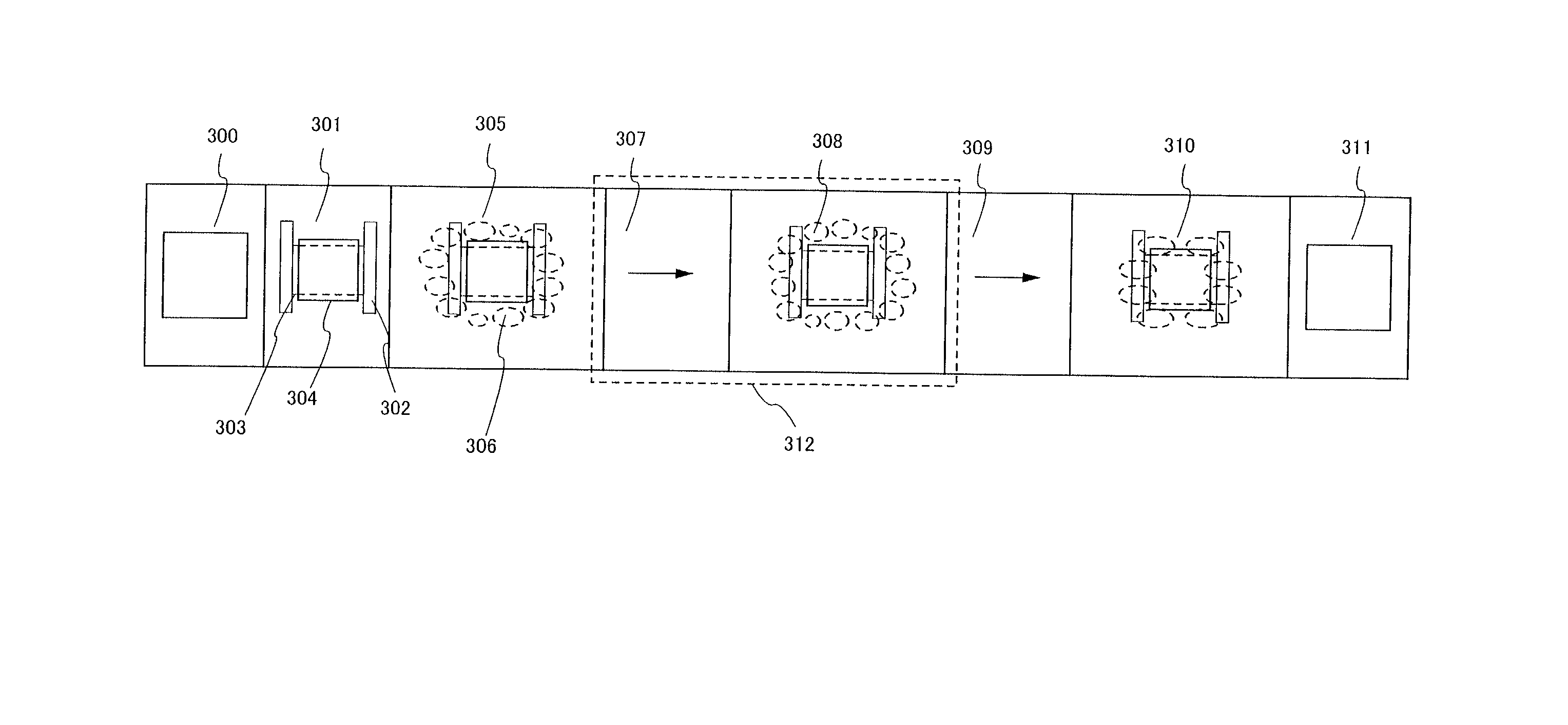
[0197] In this embodiment, a deposition apparatus will be explained with reference to FIGS. 8A and 8B, which is different in substrate transfer method and structure from the deposition apparatus of the inline type as has been indicated in the embodiment 1.

[0198] In FIGS. 8A and 8B, a substrate 804 as loaded into a load chamber 800 is transported toward a first alignment unit 801 which is coupled thereto via a gate (not shown). Note that the substrate 804 is subjected to alignment by the method discussed in FIGS. 4A through 4E and then fixed to a holder 802 along with a metal mask 803.

[0199] And, the substrate 804 is transferred to a first deposition unit 805 together with the holder 802. Note here that the first alignment unit 801 and the first deposition unit 805 are coupled together via no gates and have the same space. Then, in this embodiment, a rail 812 is provided as a means for enabling free movement between the first alignment unit 801 and the first depo...


PUM

PropertyMeasurementUnit
Coloraaaaaaaaaa
Luminescenceaaaaaaaaaa

Abstract

A deposition apparatus is provided for manufacturing an organic compound layer having a plurality of function regions. The deposition apparatus includes a plurality of evaporation sources within a deposition chamber, for enabling continuous formation of respective function regions comprised of organic compounds and, further, formation of a mixed region at an interface between adjacent ones of the function regions. With the deposition apparatus having such fabrication chamber, it is possible to prevent impurity contamination between the functions regions and further possible to form an organic compound layer with an energy gap relaxed at the interface.

Description

[0001] 1. Field of the invention[0002] The invention relates to a luminescent device using an organic luminescent element having an anode, a cathode, and a film (referred below to as "organic compound layer"), which includes an organic compound adapted to effect luminescence upon application of an electric field. Specifically, the present invention relates to a manufacturing of a luminescent element which requires a lower drive voltage and has a longer life than luminescent devices of the related art. Further, the luminescent device described in the specification of the present application indicates an image display device or a luminescent device, which use an organic luminescent element as luminescent element. Also, the luminescent device includes all of modules, in which a connector, for example, an anisotropic electroconductive film (FPC:Flexible printed circuit) or a TAB (Tape Automated Bonding) tape or a TCP (Tape Carrier Package) is mounted to an organic luminescent element, m...

Claims


Application Information

Patent Timeline
IPC IPC(8): B05D7/24C23C14/12H05B33/10C23C14/56H01L51/00H01L51/40H01L51/50H05B33/02H05B33/12
CPCB05D1/60C23C14/12H01L2924/0002C23C14/564C23C14/568H01L51/001H01L51/5012H01L51/5036H05B33/02H05B33/12H01L33/08H01L33/36H01L51/5203H01L2924/00H10K71/164H10K50/11H10K50/125A47J31/4403A47J31/06H10K50/805H10K30/865H10K50/157
Inventor YAMAZAKI, SHUNPEISEO, SATOSHIMIZUKAMI, MAYUMI
Owner SEMICON ENERGY LAB CO LTD
Why Eureka
Try Eureka