Semiconductor light-emitting device and method for manufacturing the same

a semiconductor and light-emitting technology, applied in the direction of semiconductor lasers, lasers, semiconductor laser structural details, etc., can solve the problems of reducing the light-emission efficiency or deteriorating the life characteristic, imposing an obstacle in improving the life of the element, and the drawback of the semiconductor construction of algan/ingan/gan based semiconductor, etc., to achieve the effect of improving the crystallinity of the active layer

Inactive Publication Date: 2006-11-07
ROHM CO LTD
View PDF7 Cites 188 Cited by
  • Summary
  • Abstract
  • Description
  • Claims
  • Application Information

AI Technical Summary

Benefits of technology

[0096]If a buffer layer made of an n-type ZnO-based compound semiconductor having a larger band gap energy than the activ

Problems solved by technology

Therefore, the temperature cannot be raised to a high temperature needed for obtaining a semiconductor layer having an excellent crystallinity, so that it is not possible to obtain semiconductor layers having a good crystallinity, raising a problem of reduction in the light-emission efficiency or deterioration in the life characteristic.
Further, a semiconductor laser constructed with AlGaN/InGaN/GaN based semiconductor has a drawback as an important physical property.
On the other hand, if it is doped with an impurity, it is not possible to avoid generation of a non-light emitting recombination center, so that carriers are consumed in a process other than the light emission, thereby conversely raising the threshold value and inviting the temperature rise of the element during light emission.
This imposes an obstacle in improving the life of the element, particularly in the improvement of life at the time of producing a high output.
As described above, the InGaN materials used for an active layer of a conventional blue semiconductor light emitting device have a problem that the threshold value tends to rise by the stress accompanying the lattice mismatch.
Therefore, in

Method used


Image

  • Semiconductor light-emitting device and method for manufacturing the same
  • Semiconductor light-emitting device and method for manufacturing the same
  • Semiconductor light-emitting device and method for manufacturing the same

Examples


Embodiment Construction

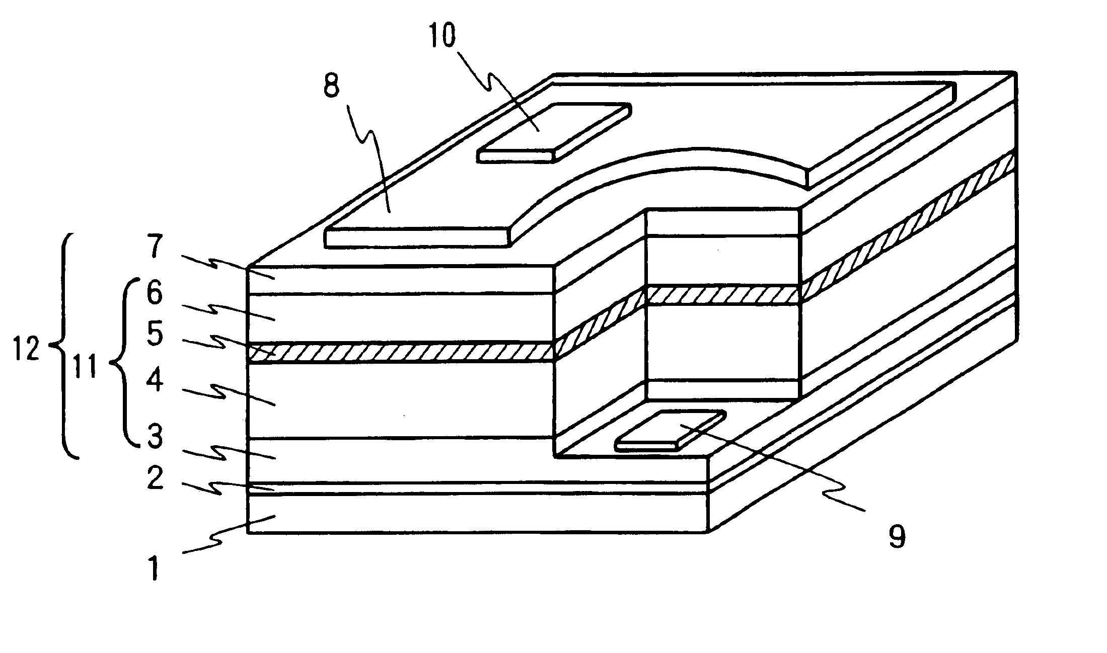
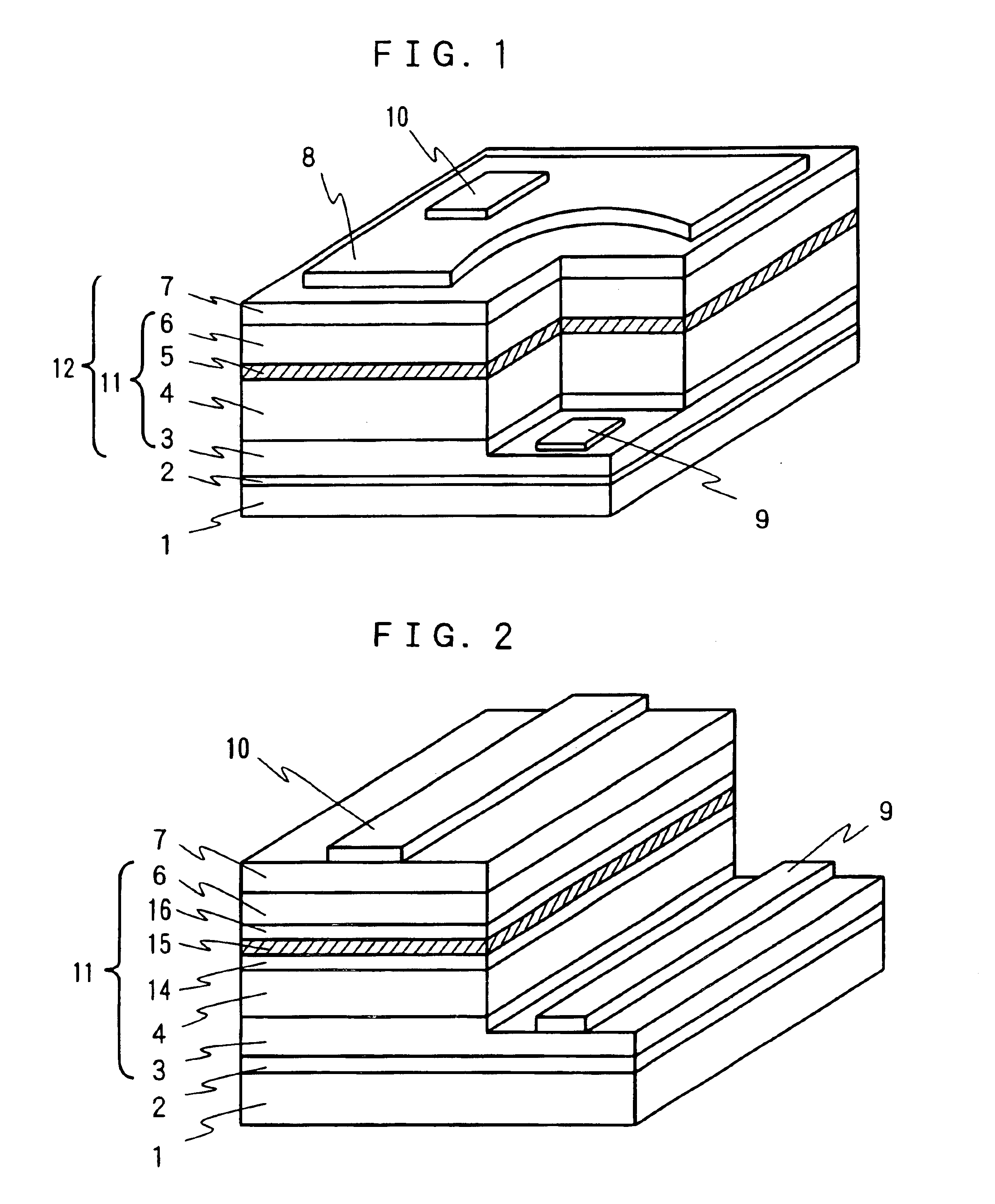
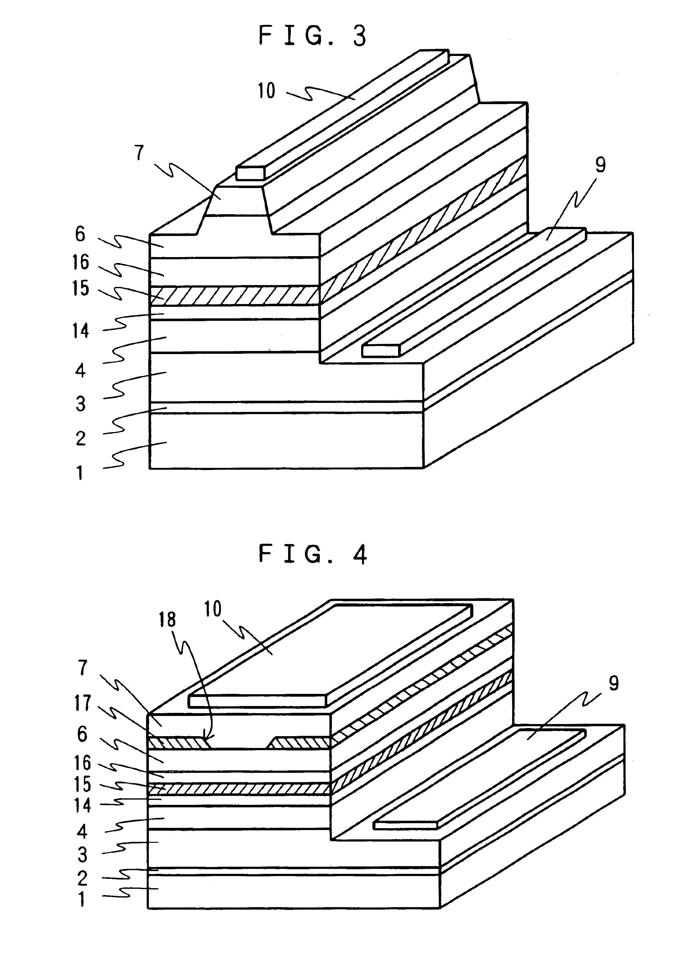
[0144]Next, a semiconductor light emitting device of the present invention will be explained with reference to the drawings.

[0145]A semiconductor light emitting device of the present invention has a structure such that an active layer 5 emitting light by electric current injection is sandwiched between an n-type cladding layer 4 and a p-type cladding layer 6 made of materials having a larger band gap than the active layer 5 as illustrated in FIG. 1 showing a perspective view of a LED chip as an embodiment thereof, and said active layer 5, is made of an oxide compound semiconductor containing at least one of Cd and Zn.

[0146]The active layer 5 is a layer for emitting light by recombination of carriers, and its band gap determines the wavelength of the emitted light. A material having a band gap that corresponds to the wavelength of the light to be emitted is used. For example, the active layer 5 is a single active layer formed to have a thickness of about 0.3 μm. The present invention...


PUM


Abstract

It has a structure in which an active layer (5) that emits light by electric current injection is sandwiched between an n-type cladding layer (4) and a p-type cladding layer (6) made of materials having a larger band gap than the active layer (5), wherein the active layer (5) is made, for example, of CdxZn1−xO (0≦x<1). It is further more preferable if the cladding layers (4), (6) are made, for example, of MgyZn1−yO (0≦y<1). This narrows the band gap of the ZnO materials, and an oxide semiconductor capable of being wet-etched, easy to handle with, and excellent in crystallinity can be used as a material for an active layer or a cladding layer of a semiconductor light emitting device such as a blue light emitting diode or a blue laser diode in which an active layer is sandwiched between cladding layers, so that a blue semiconductor light emitting device being excellent in light emission characteristics can be obtained.

Description

TECHNICAL FIELD[0001]The present invention relates to a compound semiconductor light emitting device, such as a light emitting diode or a laser diode, that emits light with a short wavelength of blue color from ultraviolet to around yellow, and a method for manufacturing the same. More particularly, the present invention relates to a semiconductor light emitting device typically made of a ZnO-based compound semiconductor and being excellent in crystallinity and easy to handle with.BACKGROUND ART[0002]A blue light emitting diode (hereinafter referred to as LED) used as a light source of full color display or a signal lamp and a blue laser diode (hereinafter referred to as LD) used as a light source of a highly fine next-generation DVD that continuously oscillates at room temperature are attracting people's attention because it has recently become possible to obtain them by lamination of GaN-based compound semiconductor on a sapphire substrate.[0003]Conventional blue semiconductor lig...

Claims


Application Information

Patent Timeline
IPC IPC(8): H01L27/15H01L21/363H01L33/06H01L33/12H01L33/28H01L33/32H01S5/02H01S5/32H01S5/327H01S5/347
CPCB82Y20/00H01L33/28H01S5/327H01L21/0237H01L21/0242H01L21/02472H01L21/02488H01L21/02554H01L21/02565H01L21/02576H01L21/02579H01L21/0262H01L21/02631H01S5/0213H01S5/0422H01S5/2224H01S5/2231H01S5/3214H01S5/34333H01S5/347
Inventor TANABE, TETSUHIRONAKAHARA, KEN
Owner ROHM CO LTD
Why Eureka
Try Eureka