

Robot arm
a robot arm and arm body technology, applied in the field of robot arms, can solve the problems of limited contamination in the interior of the transfer chamber, and achieve the effect of accurate positioning and limit contamination within the transfer chamber
- Summary
- Abstract
- Description
- Claims
- Application Information
AI Technical Summary
Benefits of technology
Problems solved by technology
Method used
Image

Examples
Embodiment Construction
[0014]Technical features of a robot arm, which will be described in the exemplary embodiment, will be briefly noted in the following.
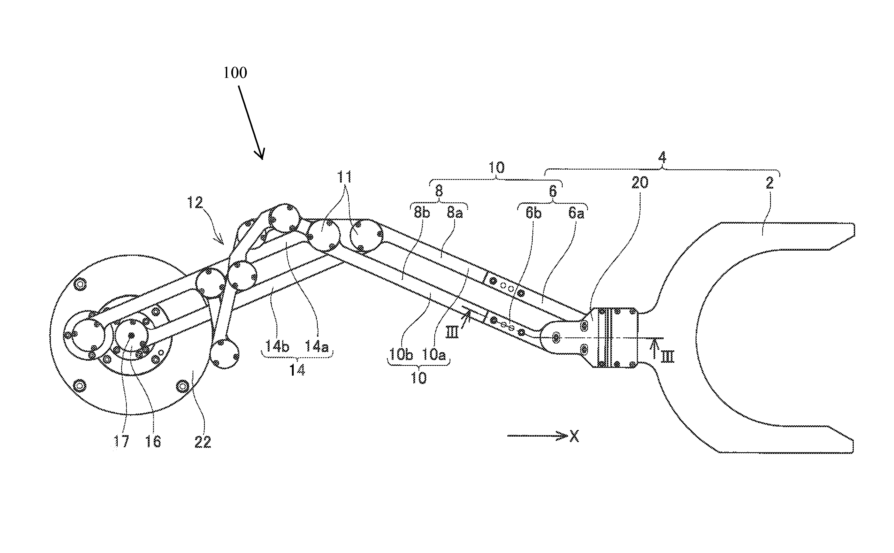
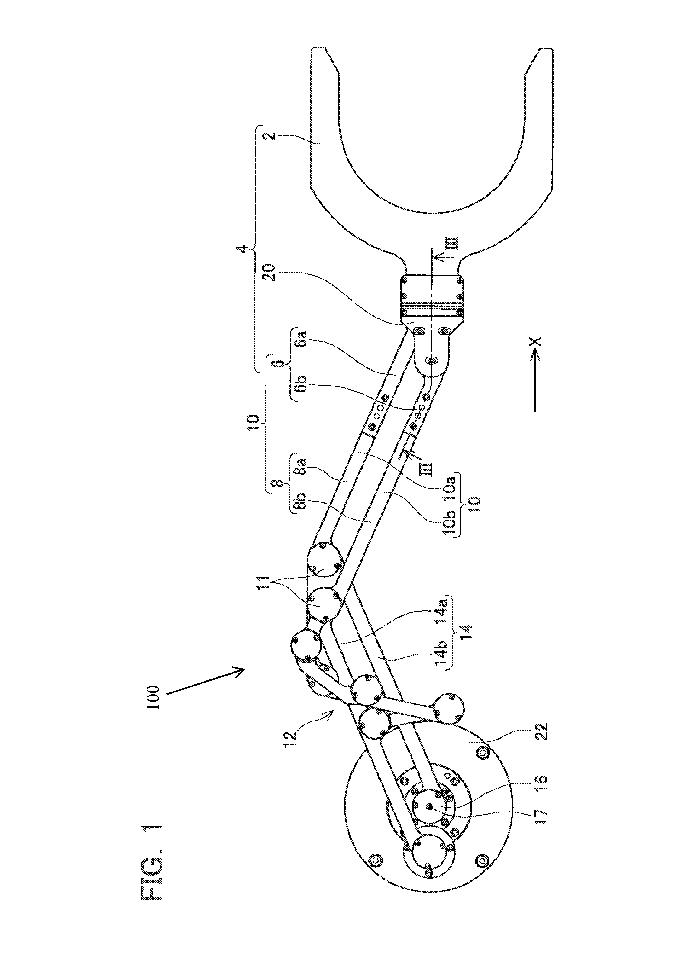
[0015](Feature 1) The robot arm is a horizontal type robot in which axial lines of a first bearing and a second bearing extend in a vertical direction, and that moves a hand in a horizontal plane.
[0016](Feature 2) The thickness of a portion where a distal end portion and a proximal end portion of a lower arm link overlap equals the thickness of a non-overlapping portion adjacent to the overlapping portion.
[0017](Feature 3) The distal end portion of the lower arm link is located on the upper side of the proximal end portion of the lower arm link.
[0018](Feature 4) The distal end portion of the lower arm link and the proximal end portion of the lower arm link are fixed by a plurality of bolts, and the plurality of bolts is disposed on both sides of positioning pins along a longitudinal direction of the lower arm link.
[0019](Feature 5) The positioning pins...
PUM
 Abstract
Description
Claims
Application Information