Method of manufacturing semiconductor device

a manufacturing method and semiconductor technology, applied in semiconductor/solid-state device manufacturing, basic electric elements, electric devices, etc., can solve the problems of reducing affecting the service life of the device, and affecting the quality of the device, so as to prevent the generation of a leak current and good quality

Inactive Publication Date: 2013-04-11
TOKYO ELECTRON LTD
View PDF6 Cites 56 Cited by
  • Summary
  • Abstract
  • Description
  • Claims
  • Application Information

AI Technical Summary

Benefits of technology

[0010]According to embodiments of the present invention, even if an organic film such as a polyimide film is used as an insulating film, degradation of an insulating property of the insulating film caused by cleaning through irradiation of plasma of an inert gas may be restored, and thus a good quality semiconductor device capable of preventing generation of a leak current may be manufactured.

Problems solved by technology

However, when an organic film such as a polyimide film is used as the insulating film formed in the hole, if such a cleaning process is performed, the organic film may be damaged due to the Ar plasma, and thus an insulating property may be degraded.

Method used


Image

  • Method of manufacturing semiconductor device
  • Method of manufacturing semiconductor device
  • Method of manufacturing semiconductor device

Examples


Embodiment Construction

[0025]Hereinafter, the present invention will be described in detail by explaining exemplary embodiments of the invention with reference to the attached drawings.

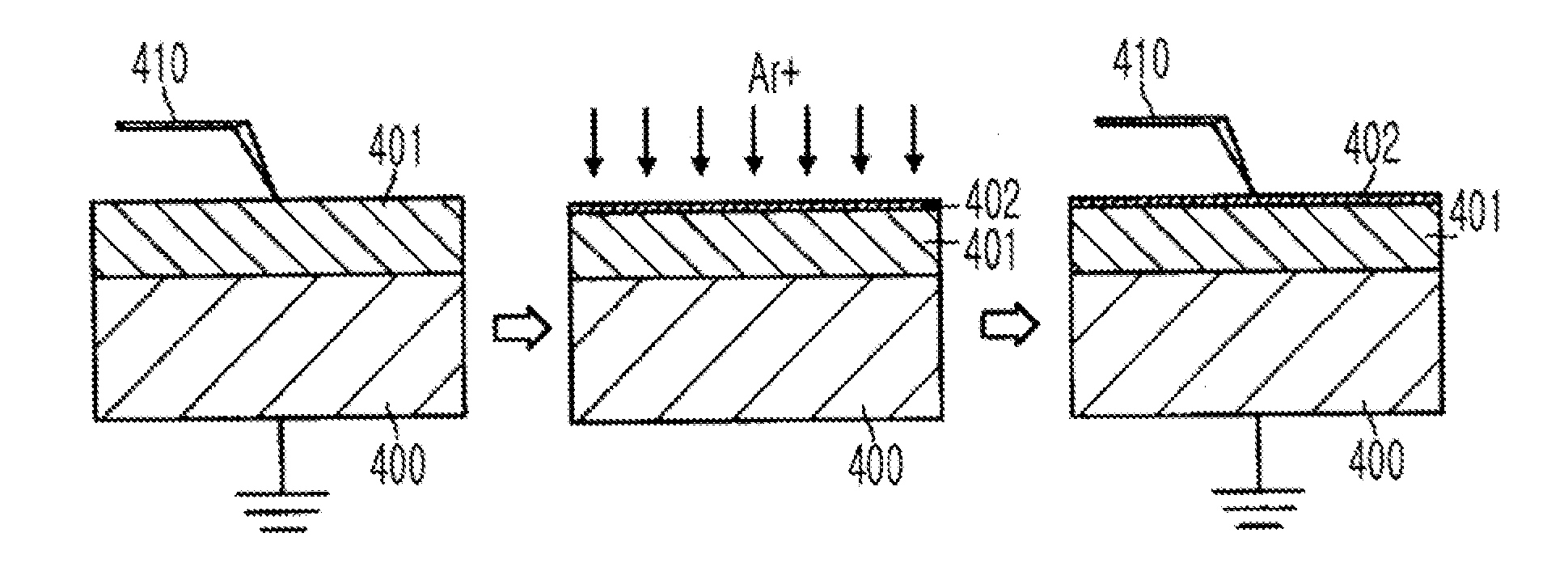
[0026]FIG. 4 is schematic views for describing a process according to an embodiment of the present invention, FIG. 4 shows a process of manufacturing a sample for measuring an insulating property of a polyimide film to be described below. As shown in part (a) of FIG. 4, a polyimide film 401 is formed on a silicon substrate 400 by evaporation polymerization.

[0027]Next, as shown in part (b) of FIG. 4, similarly to a cleaning process performed on a real semiconductor device, Ar plasma is irradiated on a surface of the polyimide film 401,

[0028]Part (c) of FIG. 4 shows a state of the polyimide film 401 after performing the cleaning process. The Ar plasma is irradiated on the surface of the polyimide film 401, and thus a layer 402 in which a change occurred, for example, an imide ring disappears, is formed on the surface of the p...


PUM


Abstract

The method includes forming a hole penetrating from one surface of a substrate to an electrode formed on the other surface of the substrate; forming an organic insulating film in the hole; removing at least a part of the organic insulating film formed in a bottom portion of the hole and not the organic insulating film formed on a side wall portion of the hole, to expose the electrode; cleaning an exposed surface of the electrode by using plasma of an inert gas; filling a conductive metal in the hole; removing at least a part of a surface of the organic insulating film by the reaction of oxygen plasma; and annealing the substrate in a dysoxidative atmosphere.

Description

TECHNICAL FIELD[0001]The present invention relates to method of manufacturing a semiconductor device.BACKGROUND ART[0002]In the manufacturing field of semiconductor devices, there have been many attempts to increase the integration of semiconductor devices by making the semiconductor smaller. Also, recently, attempts are being made to increase the integration per unit area by stacking a semiconductor device, which is referred to as three-dimensional (3D) mounting.[0003]A plurality of semiconductor devices (chips) stacked in a vertical direction include an electrode that is formed through a substrate and thus the semiconductor devices (chips) are electrically connected to one another via the electrode. When the electrode penetrating the substrate is formed, an insulating film is formed in a hole formed in the substrate, and only the insulating film formed in a bottom portion of the hole and not the insulating film formed on a side wall portion of the hole, is removed so as to expose ...

Claims


Application Information

Patent Timeline
Patent Type & Authority Applications(United States)
IPC IPC(8): H01L21/283
CPCH01L21/0206H01L21/02063H01L21/31058H01L21/31138H01L21/283H01L21/76828H01L21/76831H01L21/76898H01L21/76826
Inventor SUGITA, KIPPEIMATSUDA, KENJIHASHIMOTO, HIROYUKIHARADA, MUNEO
Owner TOKYO ELECTRON LTD
Why Eureka
Try Eureka