Array and moat isolation structures and method of manufacture
a technology of isolation structure and moat, applied in the field of semiconductor structure, can solve the problems of increasing cost and unable to avoid reactive ion etching (rie) lag
- Summary
- Abstract
- Description
- Claims
- Application Information
AI Technical Summary
Benefits of technology
Problems solved by technology
Method used
Image

Examples
Embodiment Construction
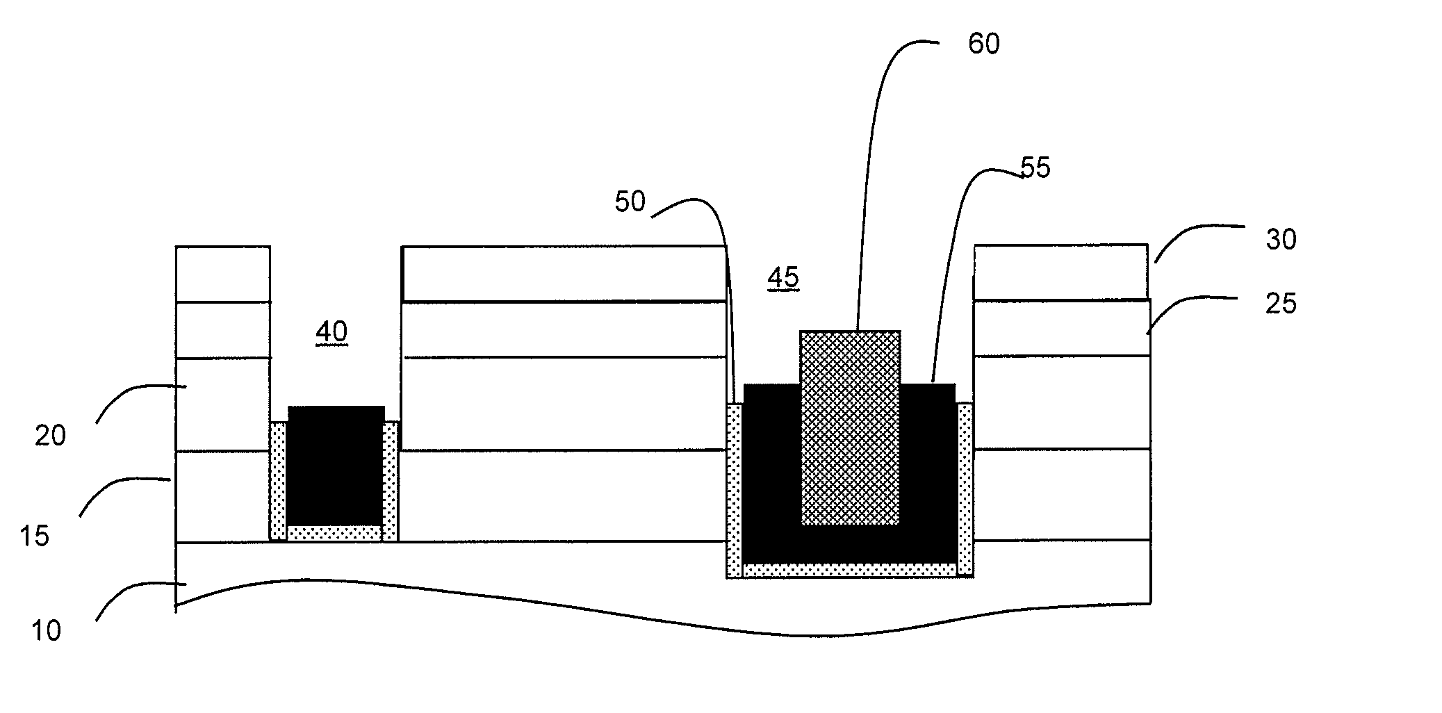
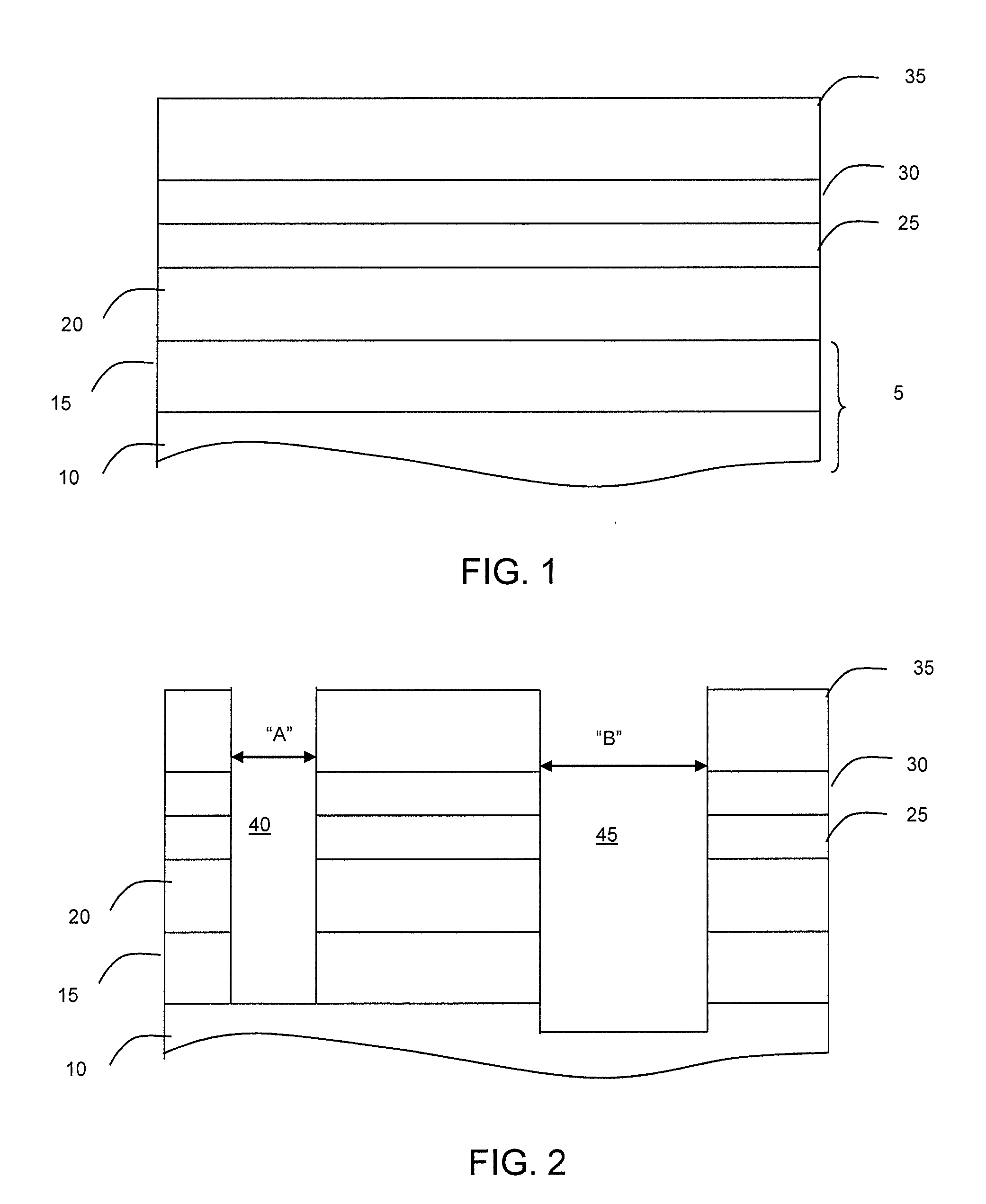
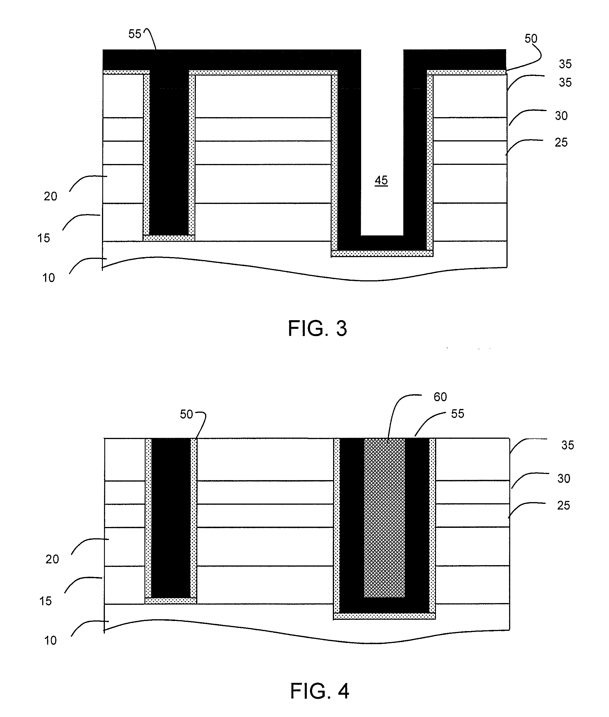
[0014]The invention relates to semiconductor structures and, more particularly, to moat isolation structures for eDRAM with heterogeneous deep trench fill and methods of manufacture. In embodiments, a deep trench for a DRAM array and moat isolation structure are filled with a metal layer. In embodiments, the metal will completely fill the deep trench of the DRAM array, while only covering sidewalls of the deep trench for the moat isolation structure. A material, e.g., Si material, then fills in the remaining portions of the moat isolation structure to form a heterogeneous deep trench fill. In embodiments, the metal deposited in the deep trench of the DRAM array is thicker than that of the metal covering sidewalls of the deep trench for the moat isolation structure. An etching process can now be performed on the metal, without any RIE lag occurring in the moat isolation structure.
[0015]Advantageously, the present invention provides improved moat isolation and eliminates or substantia...
PUM
 Abstract
Description
Claims
Application Information
 - R&D
- Intellectual Property
- Life Sciences
- Materials
- Tech Scout
- Unparalleled Data Quality
- Higher Quality Content
- 60% Fewer Hallucinations
Browse by: Latest US Patents, China's latest patents, Technical Efficacy Thesaurus, Application Domain, Technology Topic, Popular Technical Reports.
© 2025 PatSnap. All rights reserved.Legal|Privacy policy|Modern Slavery Act Transparency Statement|Sitemap|About US| Contact US: help@patsnap.com