Tape substrate with chip on film structure for liquid crystal display panel

a liquid crystal display panel and tape substrate technology, applied in the direction of electrical apparatus construction details, printed circuit non-printed electric components association, instruments, etc., can solve the problems that conventional cof (especially the output leads of conventional cof) cannot meet the high circuit density requirement for lcd panels of large size, and achieve the effect of high circuit density and wide width of conventional tape substrates

Active Publication Date: 2013-04-25
SHENZHEN CHINA STAR OPTOELECTRONICS TECH CO LTD
View PDF1 Cites 1 Cited by
  • Summary
  • Abstract
  • Description
  • Claims
  • Application Information

AI Technical Summary

Benefits of technology

[0019]In comparison with the conventional technique, the present invention can solve a problem a width of the conventional tape substrate is limited, and the conventional COF (especially the output leads of the COF) can not meet a high circuit density requirement for the LCD panel of large size.

Problems solved by technology

Therefore, obviously, the conventional COF can not meet a high circuit density requirement for the LCD panel of large size.
Accordingly, in the field of the LCD technology, it is a problem that the conventional COF (especially the output leads of the COF) can not meet the high circuit density requirement for the LCD panel of large size.

Method used


Image

  • Tape substrate with chip on film structure for liquid crystal display panel
  • Tape substrate with chip on film structure for liquid crystal display panel
  • Tape substrate with chip on film structure for liquid crystal display panel

Examples


Embodiment Construction

[0026]The following embodiments are referring to the accompanying drawings for exemplifying specific implementable embodiments of the present invention.

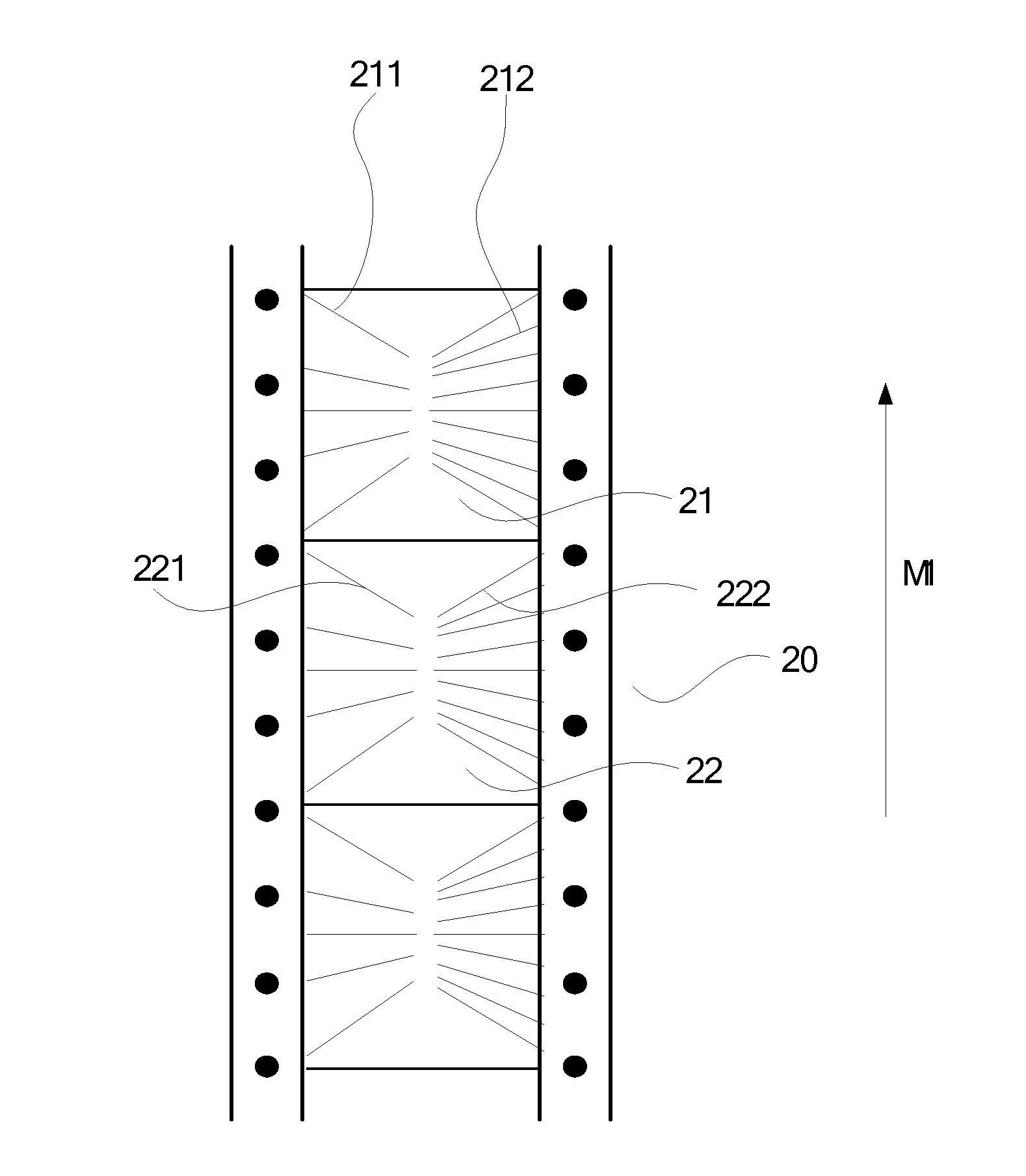
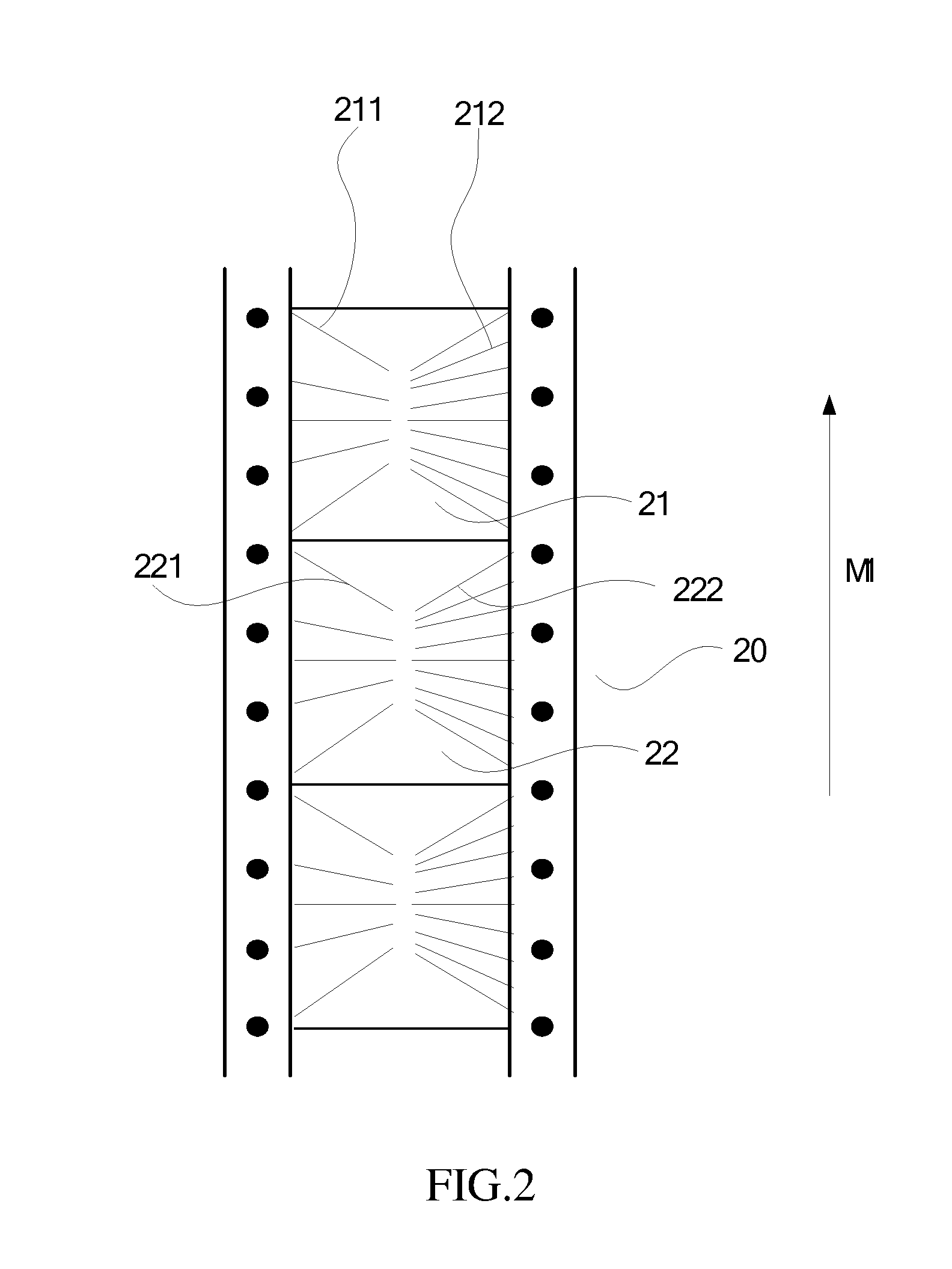
[0027]Referring to FIG. 2, FIG. 2 is a structural diagram showing a tape substrate with COF structures for a liquid crystal display panel according to a first preferred embodiment of the present invention.

[0028]The tape substrate comprises a tape substrate body 20 and a plurality of package units 21, 22 . . . with the COF structures arranged along a longitudinal direction M1 of the tape substrate body 20. Before being cut, the package units are disposed on the tape substrate body 20. In general, the tape substrate body 20 can be regarded as a flexible circuit board which comprises at least two flexible polymer layers and a circuit layer (not shown) disposed there between.

[0029]Referring to FIG. 2 again, taking the package unit 21 for example, the package unit 21 includes input leads 211 and output leads 212. In this embodiment, along...


PUM


Abstract

The present invention provides a tape substrate with COF structures for a liquid crystal display panel. A plurality of package units with the COF structures are arranged along a longitudinal direction of the tape substrate. Each of the package units includes input leads and output leads. In each of the package units, along the longitudinal direction of the tape substrate, the input leads and the output leads are disposed at both sides of the tape substrate, respectively. The present invention further provides the liquid crystal display panel using the tape substrate.

Description

FIELD OF THE INVENTION[0001]The present invention relates to a field of a liquid crystal display technology, and more particularly to a tape substrate with chip on film (COF) structures for a liquid crystal display panel and the liquid crystal display panel comprising the same.BACKGROUND OF THE INVENTION[0002]In accordance with a development of a liquid crystal display (LCD) technology, a requirement for elements of a liquid crystal display panel is raised gradually.[0003]At present, in a COF type package structure, a driving chip is basically packaged with hot press by tape automated bonding (TAB). The COF type package structure is coiled for transporting. When using the COF type package structure, COF structures can be obtained by cutting a tape substrate, and are electrically connected between a circuit on a glass substrate of an LCD panel and a driving circuit board. At least one COF structure is disposed between the glass substrate and the driving circuit board. The larger a si...

Claims


Application Information

Patent Timeline
Patent Type & Authority Applications(United States)
IPC IPC(8): H05K1/18
CPCH01L23/4985H05K1/181H01L24/50G02F1/13452H01L2924/0002H01L2924/00H01L2924/15788
Inventor LIN, POSHENLIAO, LIANGCHANWU, YU
Owner SHENZHEN CHINA STAR OPTOELECTRONICS TECH CO LTD
Why Eureka
Try Eureka