

Method and System for Generating a Photo-Response from MoS2 Schottky Junctions
a photoresponse, which is applied in the direction of transistors, semiconductor devices, electrical apparatus, etc., can solve the problem that the technology of mos2 schottky junction remains largely unexplored
- Summary
- Abstract
- Description
- Claims
- Application Information
AI Technical Summary
Benefits of technology
Problems solved by technology
Method used
Image

Examples
Embodiment Construction
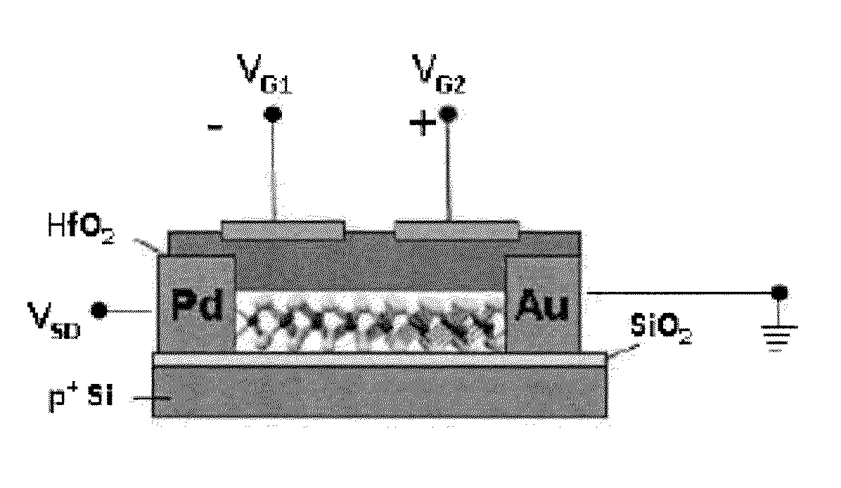
[0003]The embodiments described herein are generally directed to components incorporating molybdenum disulfide (MoS2).
[0004]2. Description of the Related Art
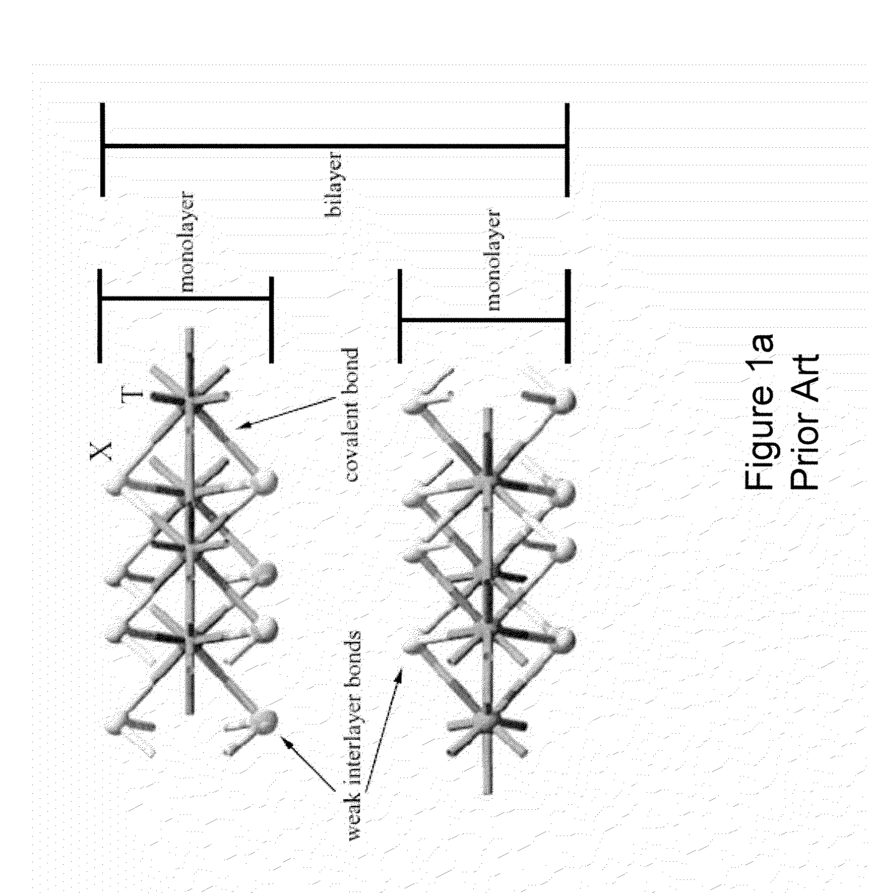
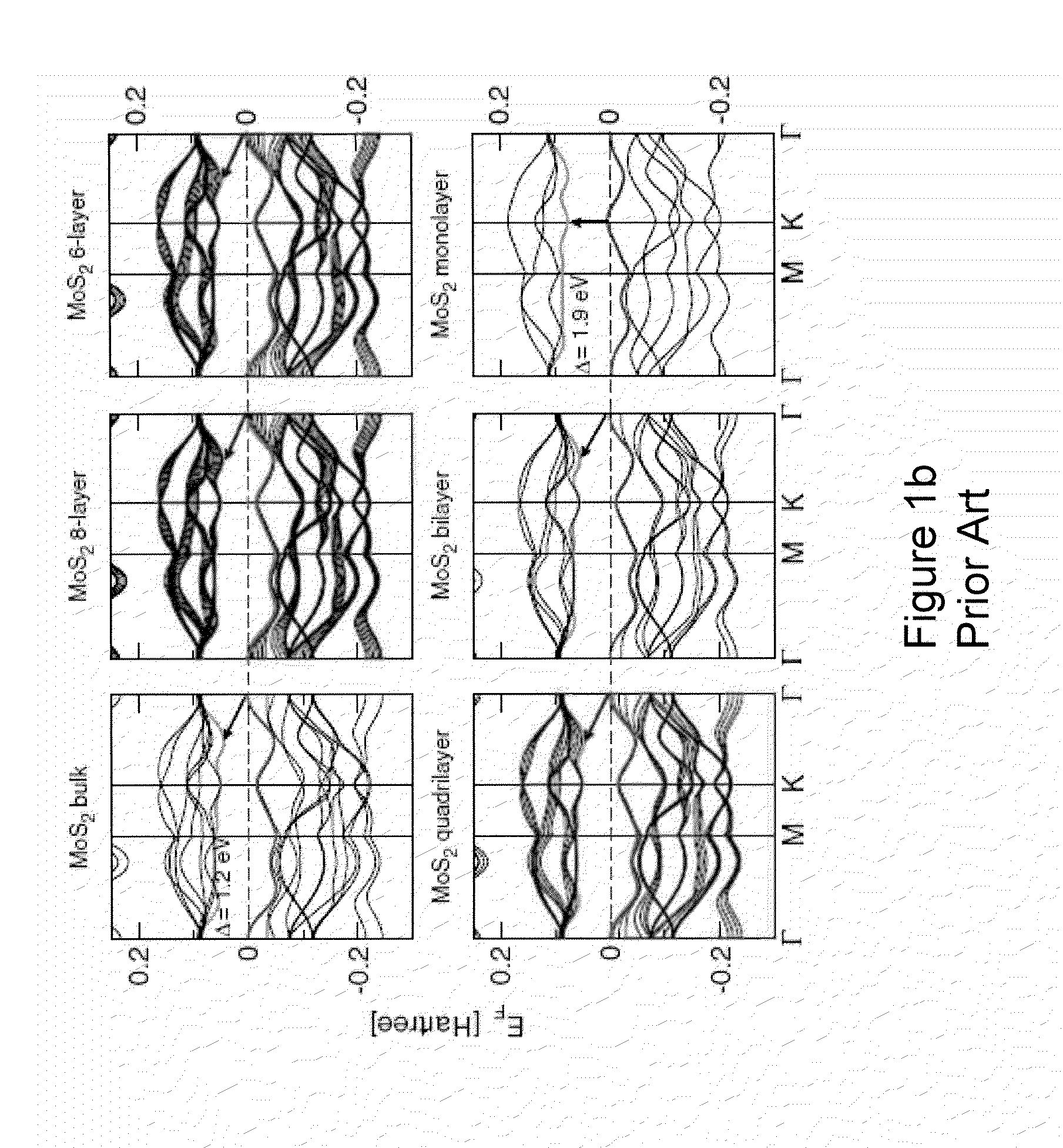
[0005]MoS2 is a semiconductor made of layers that are weakly coupled by van der Waals forces and can be easily separated via chemical or mechanical exfoliation to obtain few-layer or single-layer samples. A layer is made of three atomic planes that are strongly bonded to each other: two hexagonal planes of sulfur atoms separated by one hexagonal plane of molybdenum atoms, with each molybdenum atom covalently bonded to six sulfur atoms in the adjacent planes (see FIG. 1a Layered structure of MoS2, where X represents a S atom and T a Mo atom). Additional description may be found in A. Kuc et al., Influence of quantum confinement on the electronic structure of the transition metal sulfide TS(2), Physical Review B, 83 (2011) which is incorporated herein by reference. FIG. 1b illustrates the effect of quantum confinement on the band ...
PUM
 Abstract
Description
Claims
Application Information