
Eureka
For R&D, Eureka makes reading and utilizing patents & technical documents easy.
Eureka AIR
Designed for self-driven R&D workflows. Generate viable solutions, solve complex R&D challenges, empower your innovation with AI.

Eureka Materials
Designed for material experts only. Revolutionize your material R&D, from search, analyze, to developing new materials.

TechResearch
Generate reliable direction feasibility study reports for your R&D in just a few steps.

TechSeek
Discover and master advanced knowledge NOW. Basics, ideas, possibilities, all at once.

TechMind
As an expert in R&D Theories, TechMind can generates customized viable solutions instantly.

TechRisk
Analyze your overall solution with one click, know your potential R&D risks in advance.

TechMonitor
Get weekly tech updates, stay abreast of the latest tech innovations and key insights.
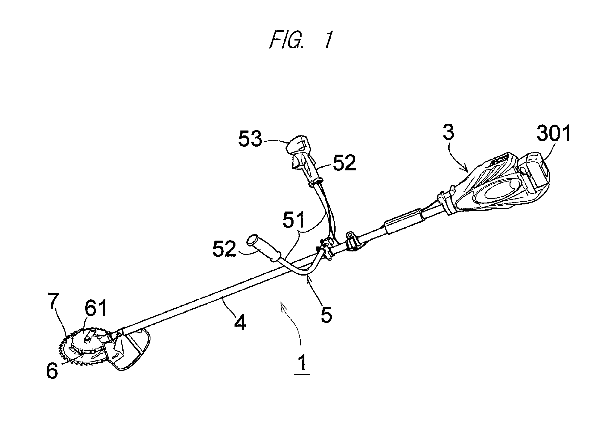
Disk motor and electric power tool equipped with the same
- Summary
- Abstract
- Description
- Claims
- Application Information
AI Technical Summary
Benefits of technology
Problems solved by technology
Method used
Image

Examples
first embodiment
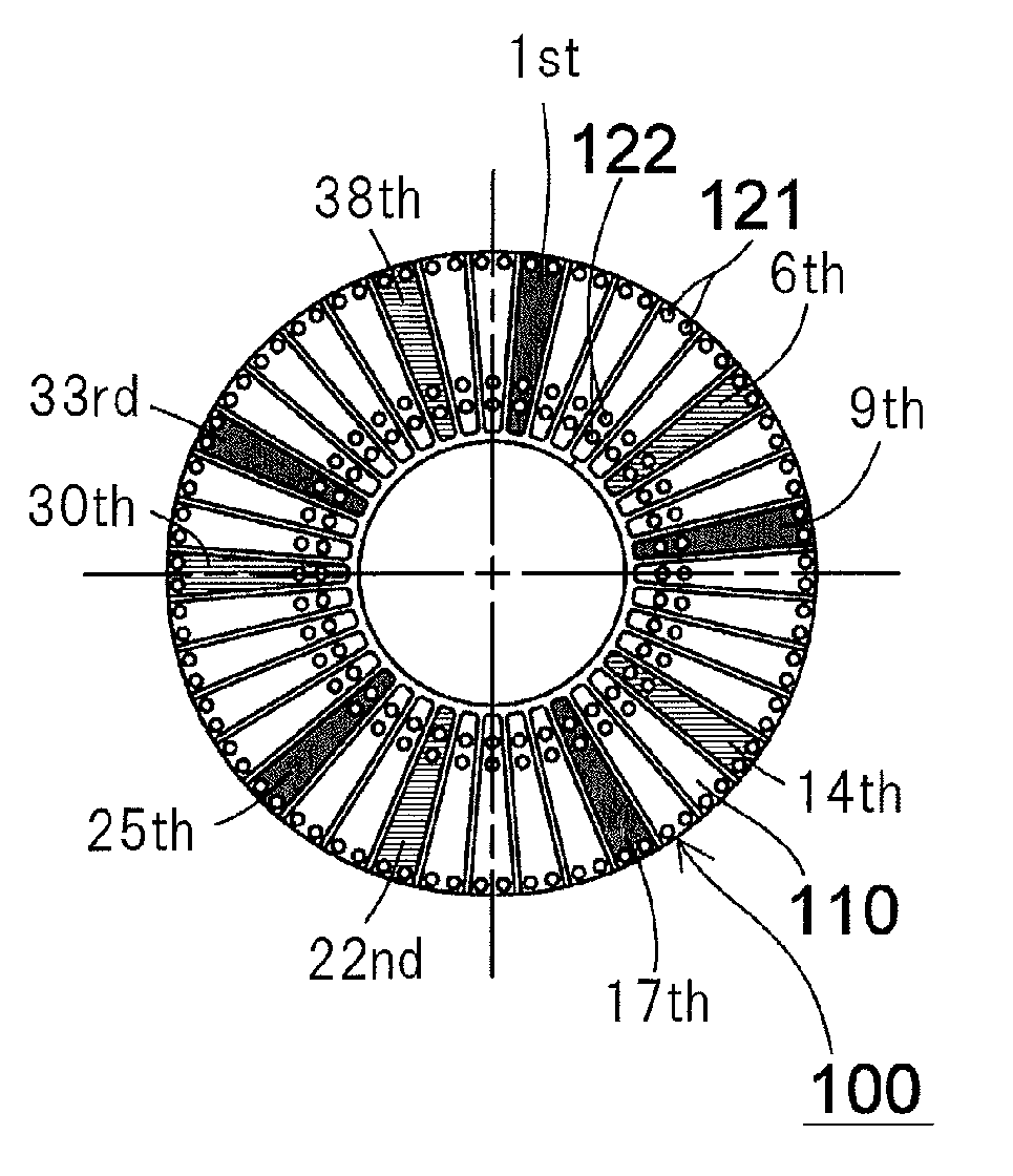
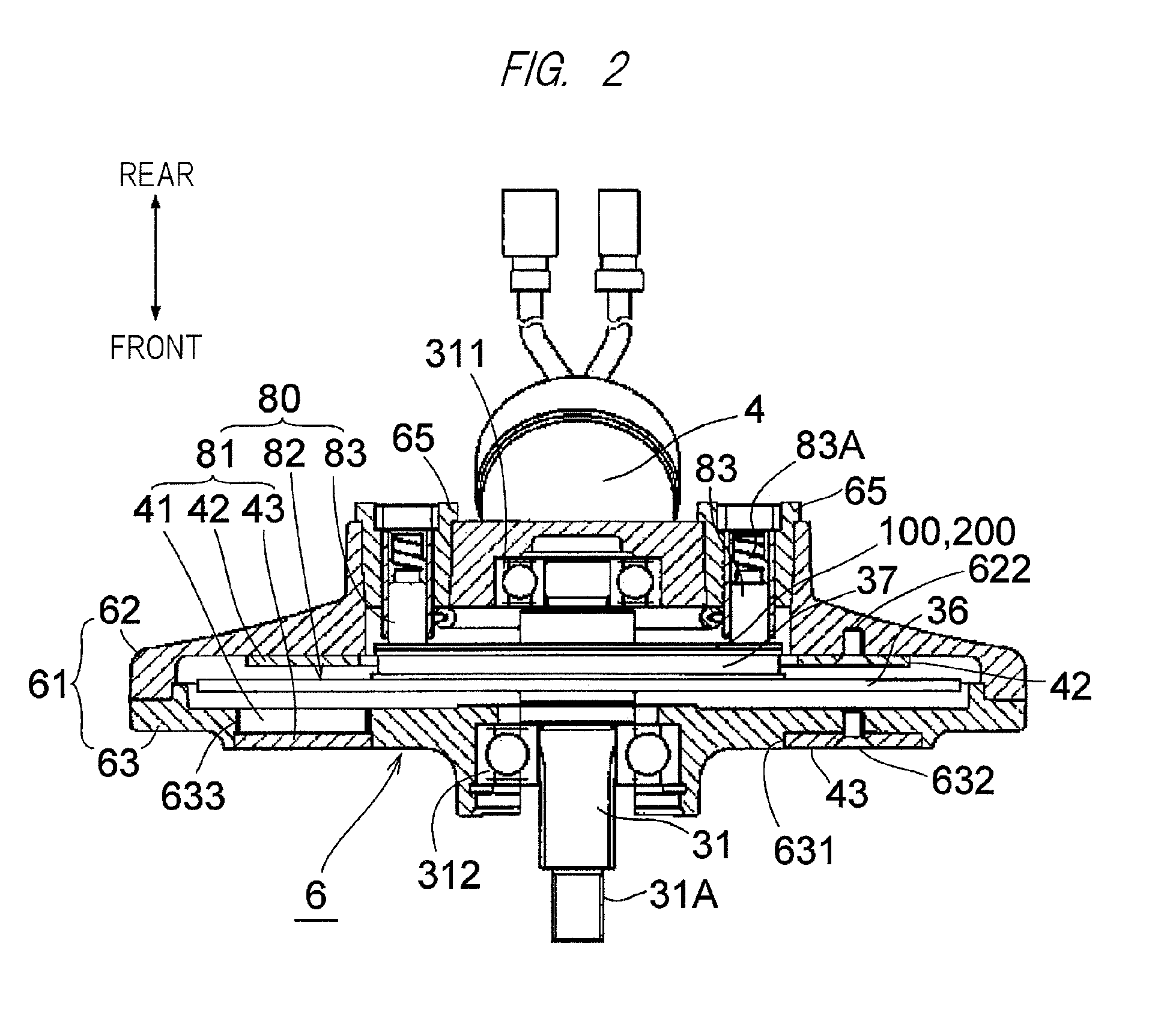
[0060]FIG. 5A is a plan view showing electrode patterns on a rear surface side of a commutator disk according to a first embodiment,
[0061]FIG. 5B is a plan view of communication patterns on a front surface side of the commutator disk transparently viewed from the rear surface side while omitting electrode patterns and an insulating substrate, and FIG. 5C is a plan view showing a front surface side of the commutator disk. The commutator disk 100 is formed by providing predetermined conductor patterns made of a conductive material such as copper on both surfaces of a disk-like insulating substrate having an opening formed at the center thereof. The insulating substrate is formed of, for example, insulating resin such as a glass-fiber reinforced epoxy resin substrate. Details of the conductor patterns will be described later.
[0062]FIG. 6A is a plan view showing communication patterns on a rear surface side of a connection disk according to the first embodiment, FIG. 6B is a plan view o...
second embodiment
[0076]FIG. 7A is a plan view showing electrode patterns on a rear surface side of a commutator disk according to a second embodiment,
[0077]FIG. 7B is a plan view of communication patterns on a front surface side of the commutator disk transparently viewed from the rear surface side while omitting electrode patterns and an insulating substrate, and FIG. 7C is a plan view showing the front surface side of the commutator disk.
[0078]FIG. 8A is a plan view showing communication patterns on a rear surface side of a connection disk according to the second embodiment, FIG. 8B is a plan view of communication patterns on a front surface side of the connection disk transparently viewed from the rear surface side while omitting communication patterns on the rear surface side and an insulating substrate, and FIG. 8C is a plan view showing the front surface side of the connection disk. Different points from the first embodiment will be mainly described below, and descriptions of points in common ...
third embodiment
[0087]FIG. 9A is a plan view showing communication patterns on a rear surface side of a connection disk according to a third embodiment, FIG. 9B is a plan view of communication patterns on a front surface side of the connection disk transparently viewed from the rear surface side while omitting the communication patterns on the rear surface side and an insulating substrate, and FIG. 9C is a plan view showing a front surface side of the connection disk.
[0088]In this embodiment, since the commutator disk 110 is equal to that of the second embodiment, illustration and description thereof are omitted. Different points from the second embodiment will be mainly described below, and description of points in common with the second embodiment will be properly omitted.
[0089]As shown in FIG. 9A, a plurality of rear-surface-side first communication patterns 251 are provided on a rear surface of a connection disk 200. As shown in FIGS. 9B and 9C, a plurality of front-surface-side first communica...
PUM
 Abstract
Description
Claims
Application Information
 - R&D Engineer
- R&D Manager
- IP Professional
- Industry Leading Data Capabilities
- Powerful AI technology
- Patent DNA Extraction
Browse by: Latest US Patents, China's latest patents, Technical Efficacy Thesaurus, Application Domain, Technology Topic, Popular Technical Reports.
© 2024 PatSnap. All rights reserved.Legal|Privacy policy|Modern Slavery Act Transparency Statement|Sitemap|About US| Contact US: help@patsnap.com