
Multilayered ceramic electronic component and fabrication method thereof

a technology of electronic components and ceramics, applied in the direction of fixed capacitor details, generators/motors, fixed capacitors, etc., can solve the problems of degrading insulation resistance and reliability, and the problem of increasing the difficulty of manufacturing, so as to prevent impurities from infiltrating

Active Publication Date: 2013-05-02
SAMSUNG ELECTRO MECHANICS CO LTD
View PDF7 Cites 26 Cited by
  • Summary
  • Abstract
  • Description
  • Claims
  • Application Information

AI Technical Summary

Benefits of technology

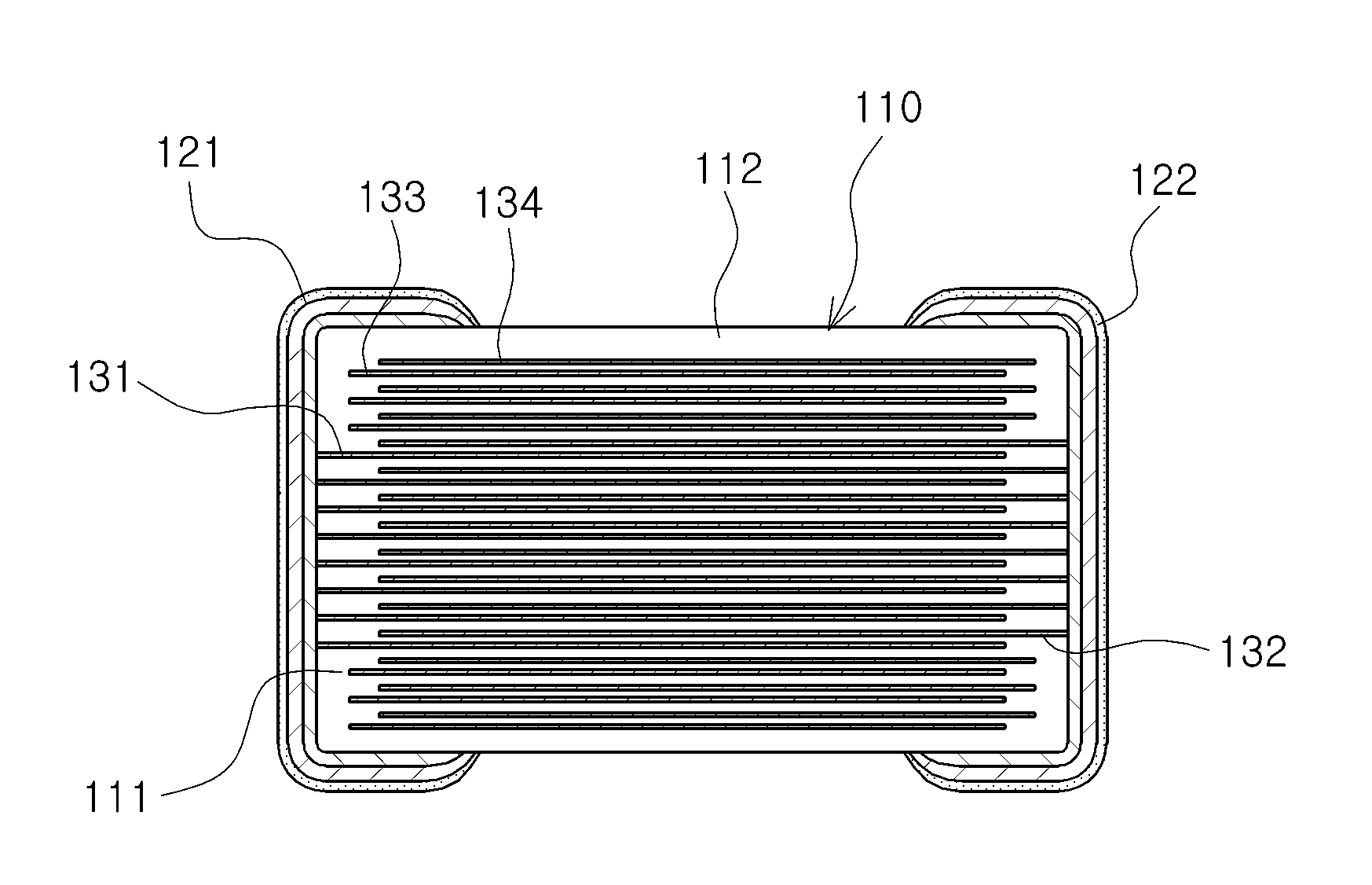
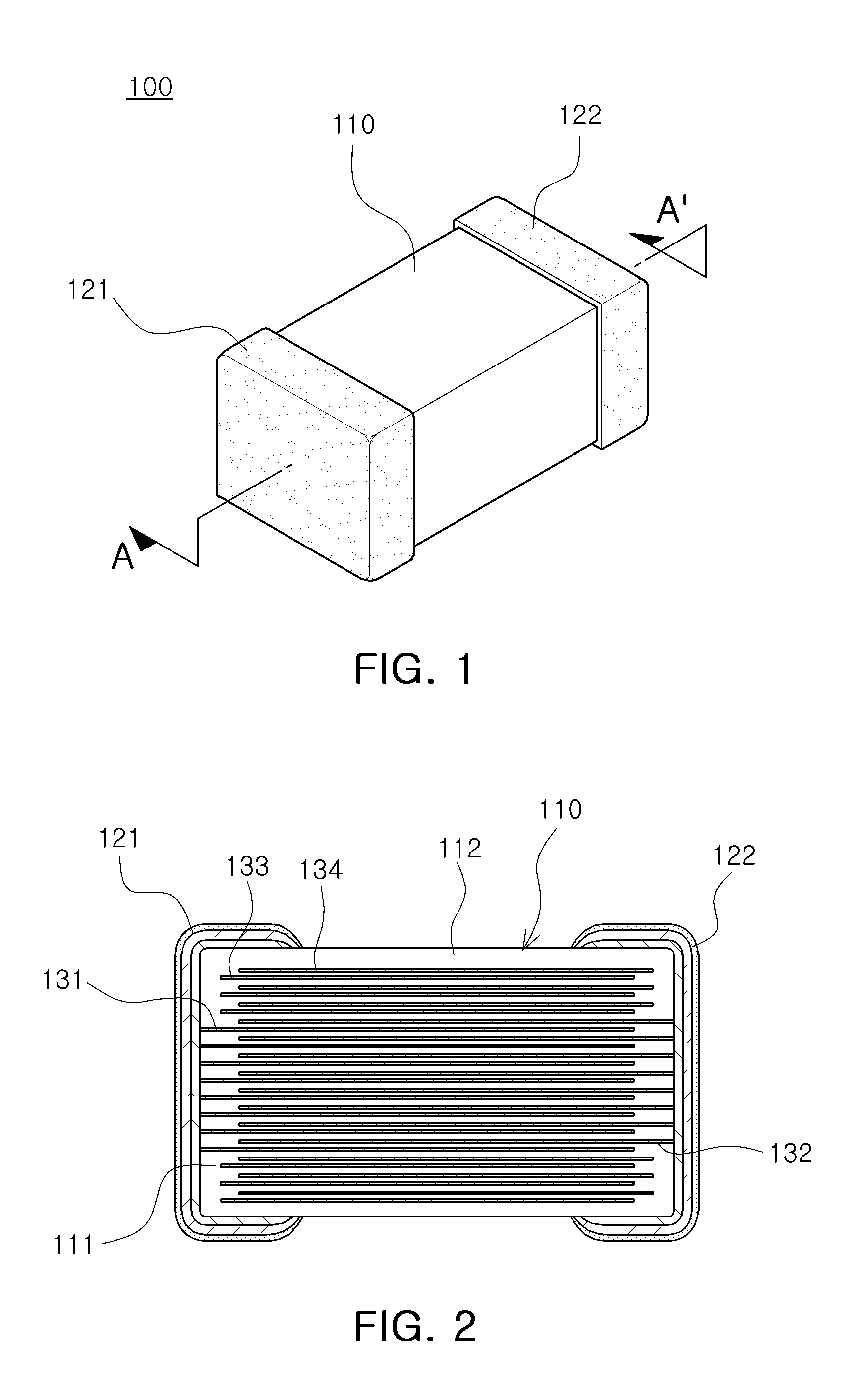
This invention provides a ceramic electronic component that can keep out impurities from entering through the corners where the inner electrodes are exposed.

Problems solved by technology

Thus, impurities such as a conductive foreign object, moisture, ions, or the like, may infiltrate through corner portions of the inner electrode having a relatively small thickness in comparison to a central portion thereof on the surface exposing the inner electrode, to degrade insulation resistance and reliability.
Such problems may become more severe in a multilayered ceramic capacitor in which a cover layer has a small thickness and a margin portion has a narrow width.

Method used


Image

  • Multilayered ceramic electronic component and fabrication method thereof
  • Multilayered ceramic electronic component and fabrication method thereof
  • Multilayered ceramic electronic component and fabrication method thereof

Examples


Embodiment Construction

[0039]Embodiments of the present invention will be described in detail with reference to the accompanying drawings.

[0040]The invention may, however, be embodied in many different forms and should not be construed as being limited to the embodiments set forth herein.

[0041]Rather, these embodiments are provided so that this disclosure will be thorough and complete, and will fully convey the scope of the invention to those skilled in the art.

[0042]In the drawings, the shapes and dimensions may be exaggerated for clarity, and the same reference numerals will be used throughout to designate the same or like components.

[0043]The same reference numerals are used for parts having similar functions and operations throughout the specification.

[0044]Throughout the specification, unless explicitly described to the contrary, the word “comprise” and variations such as “comprises” or “comprising” will be understood to imply the inclusion of stated elements but not the exclusion of any other elemen...


PUM

PropertyMeasurementUnit
Fractionaaaaaaaaaa
Fractionaaaaaaaaaa
Fractionaaaaaaaaaa

Abstract

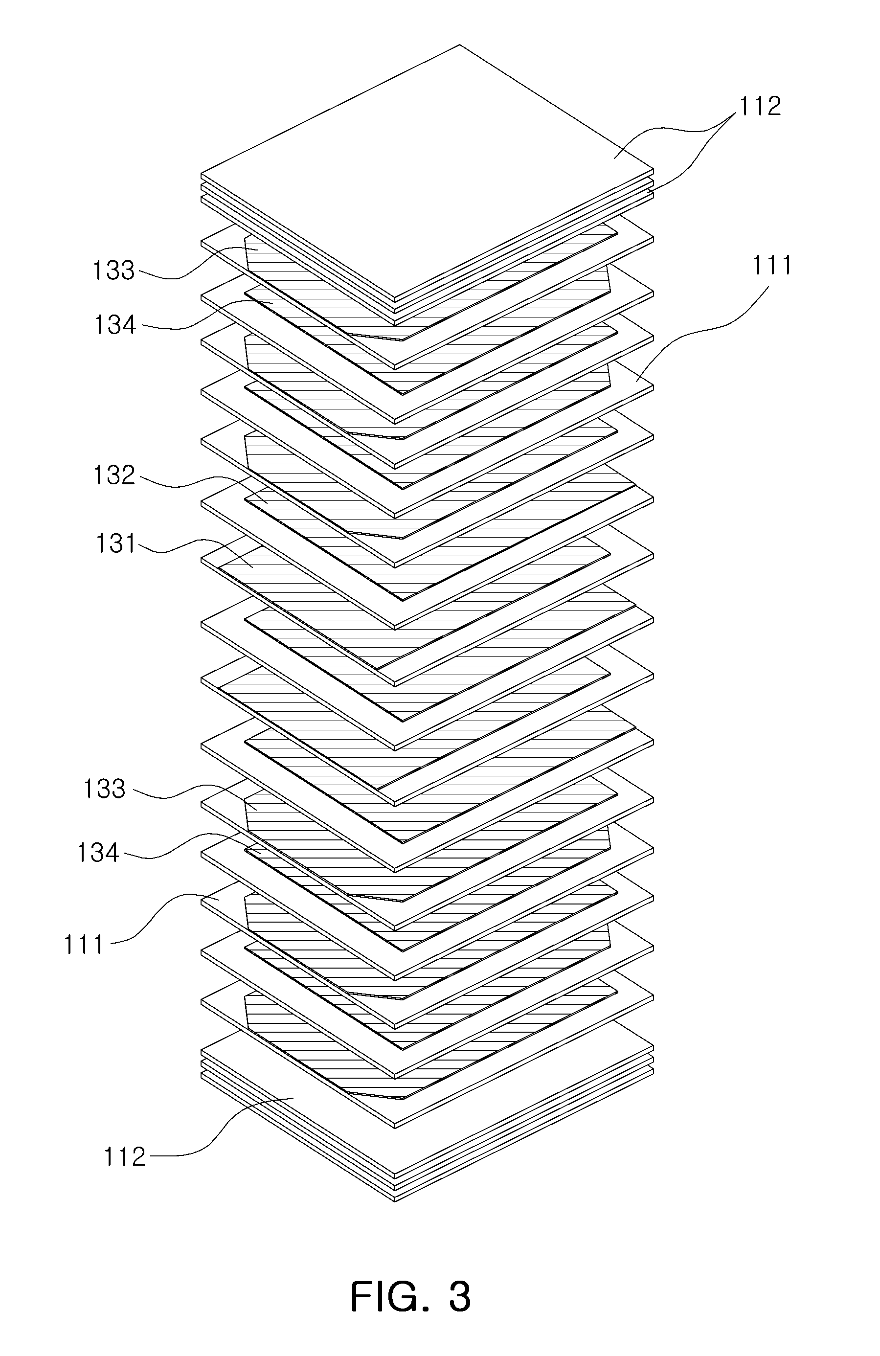
A multilayered ceramic electronic component includes: a ceramic element having a plurality of dielectric layers laminated therein; first inner electrodes formed on the dielectric layers disposed in upper and lower portions in the ceramic element, the width of a portion of each of the first inner electrodes exposed from one end face of the ceramic element being less than that of a portion thereof disposed within the ceramic element; and second inner electrodes formed on the dielectric layers disposed in the middle portion in the ceramic element, the width of a portion of each of the second inner electrodes exposed from one end face of the ceramic element being equal to that of a portion thereof disposed within the ceramic element.

Description

CROSS-REFERENCE TO RELATED APPLICATIONS[0001]This application claims the priority of Korean Patent Application No. 10-2011-0113546 filed on Nov. 2, 2011, in the Korean Intellectual Property Office, the disclosure of which is incorporated herein by reference.BACKGROUND OF THE INVENTION[0002]1. Field of the Invention[0003]The present invention relates to a multilayered ceramic electronic component and a fabrication method thereof.[0004]2. Description of the Related Art[0005]Electronic components using a ceramic material include capacitors, inductors, piezoelectric elements, varistors, thermistors, and the like.[0006]Among ceramic electronic components, a multilayered ceramic capacitor has the advantages of being small, guaranteeing high capacity, and being easily mounted.[0007]The multilayered ceramic capacitor is a chip type condenser mounted on a circuit board of various electronic products such as computers, personal digital assistants (PDAs), mobile phones, and the like, to play a...

Claims


Application Information

Patent Timeline
IPC IPC(8): H01G4/12C03B29/00H01L41/047H01C7/10H01F5/00
CPCH01C7/10H01G4/12H01C7/008H01L41/273H01G4/30H01L41/0471H01G4/005H10N30/871H10N30/053
Inventor LEE, CHUNG EUNCHOI, JAE YEOLKIM, DOO YOUNGKIM, WI HEON
Owner SAMSUNG ELECTRO MECHANICS CO LTD
Learn More