

Package Substrate Structure
- Summary
- Abstract
- Description
- Claims
- Application Information
AI Technical Summary
Benefits of technology
Problems solved by technology
Method used
Image

Examples
Embodiment Construction
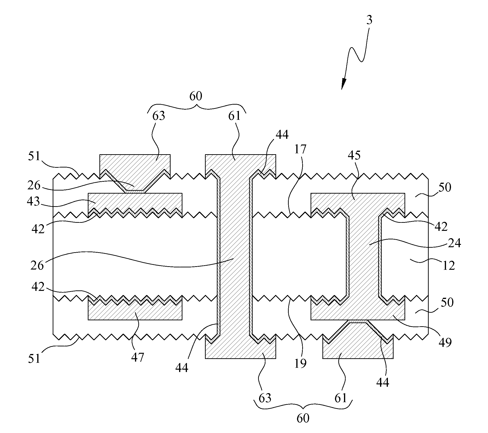
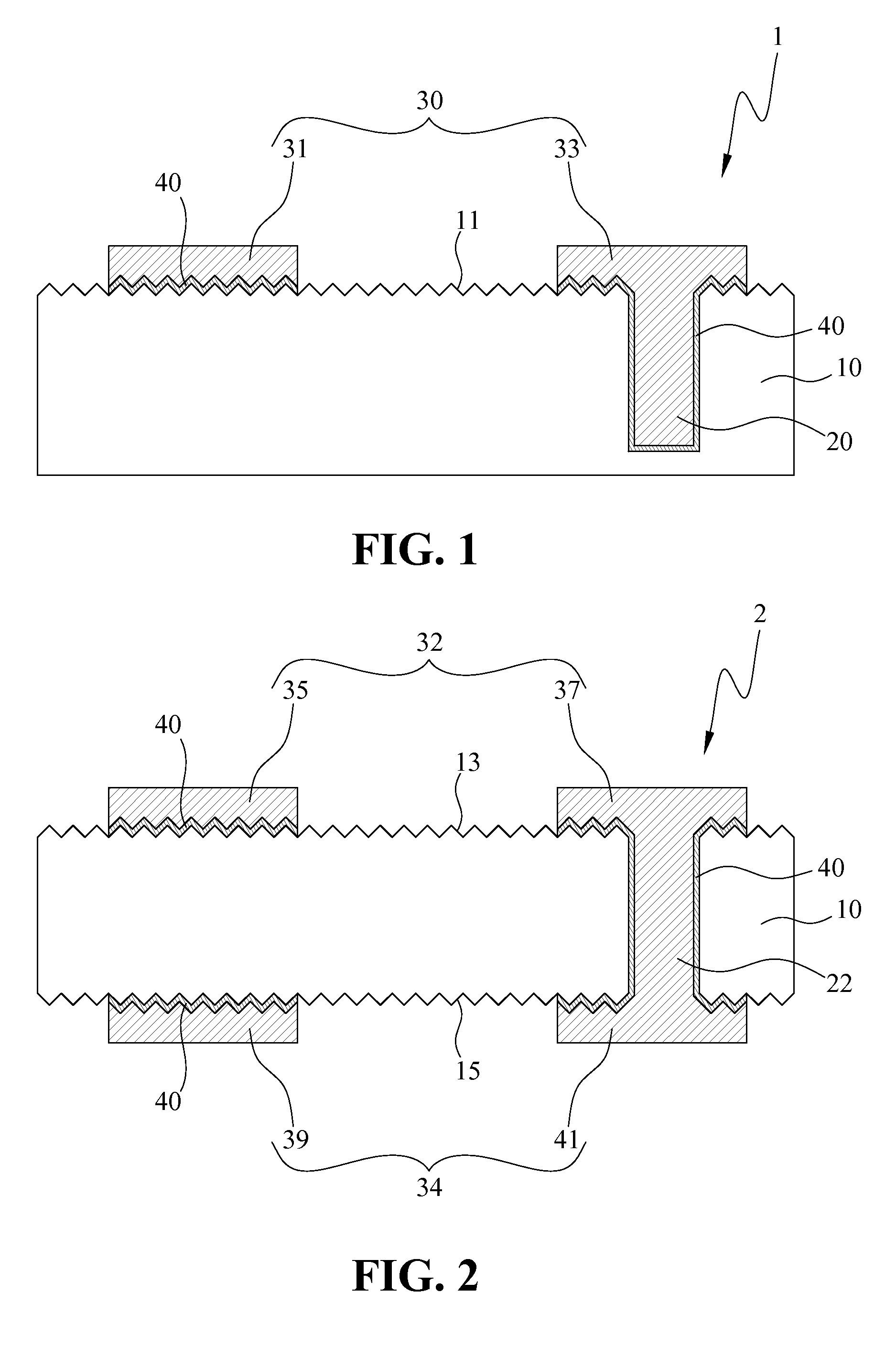
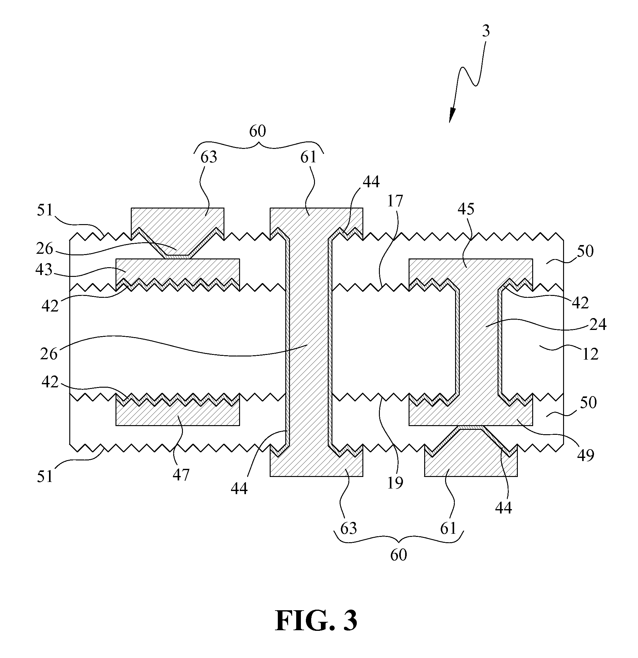
[0013]Referring to FIG. 1, a monolayer package substrate structure 1 according to the present invention comprises a substrate 10, an ultra thin seed layer 40, and a circuit layer 30. The substrate 10 has a substrate surface 11, and has at least one via hole 20 is formed therein. The ultra thin seed layer 40 is made of electrically conductive material, and is formed on portions of the substrate surface and on a sidewall and a bottom of the at least one via hole 20. The circuit layer 30 includes a plurality of metal bumps 31 and 33 wherein the metal bump 31 is formed on the ultra thin seed layer 40 formed on the portions of the substrate surface 11, and the metal bump 33 is formed on the at least one via hole 20 filled with a metallic material. In this embodiment, the ultra thin seed layer 40 is formed between the substrate surface 11 and the plurality of metal bumps 31 and 33, and also formed between the sidewall and the bottom of the at least one via hole 20, and the metallic materi...
PUM
 Abstract
Description
Claims
Application Information