Trench silicide and gate open with local interconnect with replacement gate process

a technology of local interconnection and trench contact, which is applied in the direction of semiconductor devices, electrical equipment, transistors, etc., can solve the problems of difficult bidirectional local interconnection patterning, easy failure of misalignment, and most replacement gate process that is not self-aligned, etc., to reduce the number of resistive interfaces, reduce the potential for misalignment, and improve the manufacturing yield

Active Publication Date: 2013-05-16
ADVANCED MICRO DEVICES INC
View PDF14 Cites 55 Cited by
  • Summary
  • Abstract
  • Description
  • Claims
  • Application Information

AI Technical Summary

Benefits of technology

[0020]Providing the self-aligned trench contacts extended above the gate allows a simpler local interconnect scheme to be utilized to connect to the trench contacts and an open gate. Using the process embodiments described herein may allow lower gate to trench contact and local interconnect coupling capacitance as well as reduction in the number of resistive interfaces between layers as compared to previous replacement gate flow connection schemes. In addition, process embodiments described herein may provide a better manufacturing yield by reducing the potential for misalignments between contacts and providing a simpler process flow than previous replacement gate flow connection schemes.

Problems solved by technology

Additionally, most replacement gate processes suffer from alignment issues when making trench contacts and / or local interconnect connections to the gate.
For example, most replacement gate processes are not self-aligned and can easily fail from misalignment during processing.
It may also be difficult to pattern bidirectional local interconnect and / or reduce the number of interface layers from the local interconnect to either the gate or the source / drain of the gate.
Such process flows, however, are typically very complex, have many resistive interfaces, and have high manufacturing costs due to the complex process flow.
Additionally, there is a low manufacturing margin for misalignments or other errors due to the complexity of the processes as these processes may have severely restrictive design and / or alignment rules.
In addition, there may easily be alignment issues between local interconnect 68C and gate 56′ without restrictive alignment rules.
The numerous process steps may increase the likelihood of resistive interfaces forming between the local interconnects and / or alignment issues between the local interconnects.

Method used


Image

  • Trench silicide and gate open with local interconnect with replacement gate process
  • Trench silicide and gate open with local interconnect with replacement gate process
  • Trench silicide and gate open with local interconnect with replacement gate process

Examples


Embodiment Construction

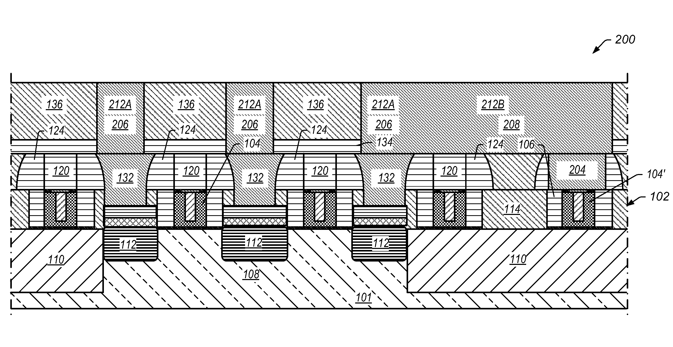
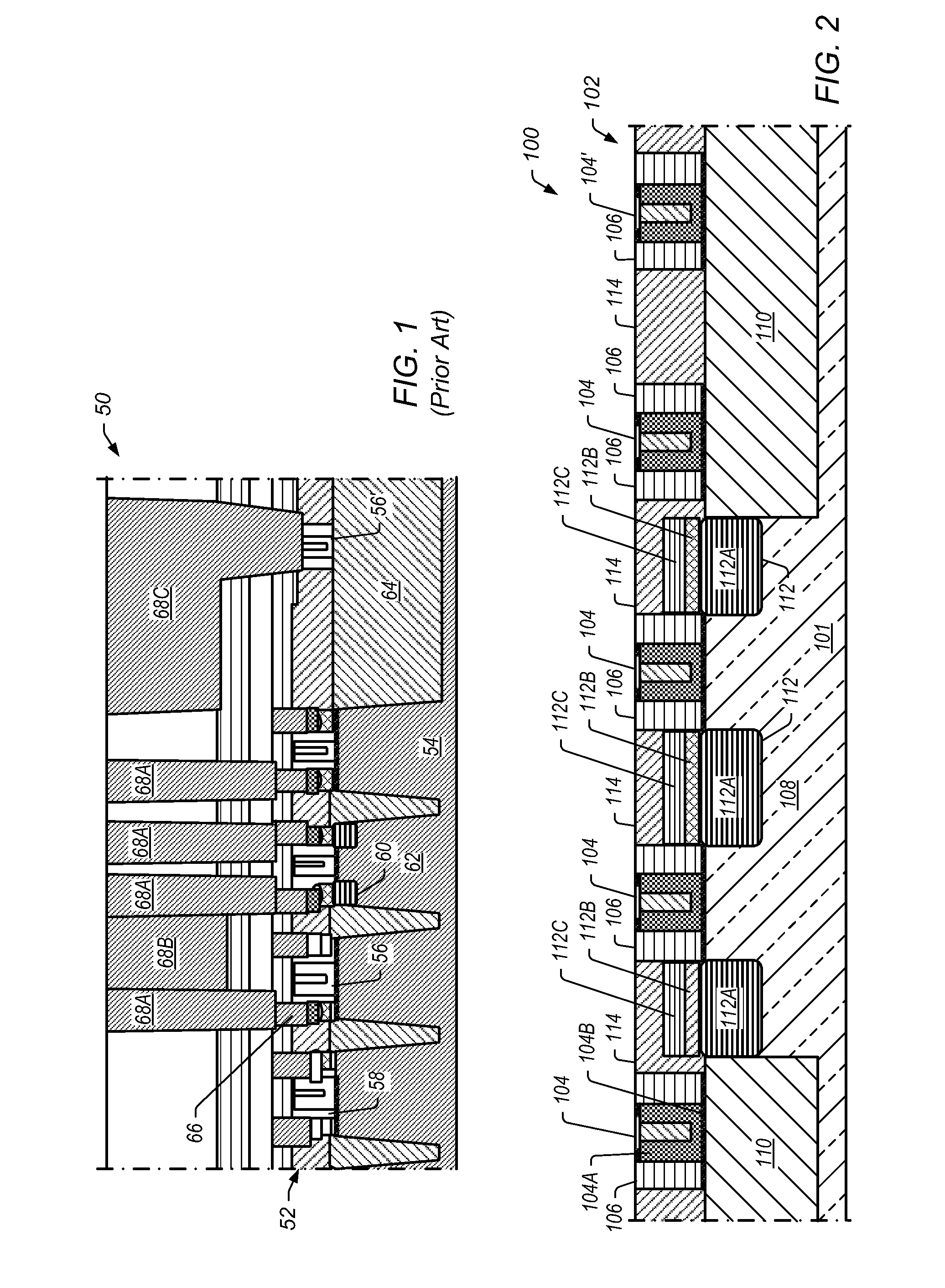
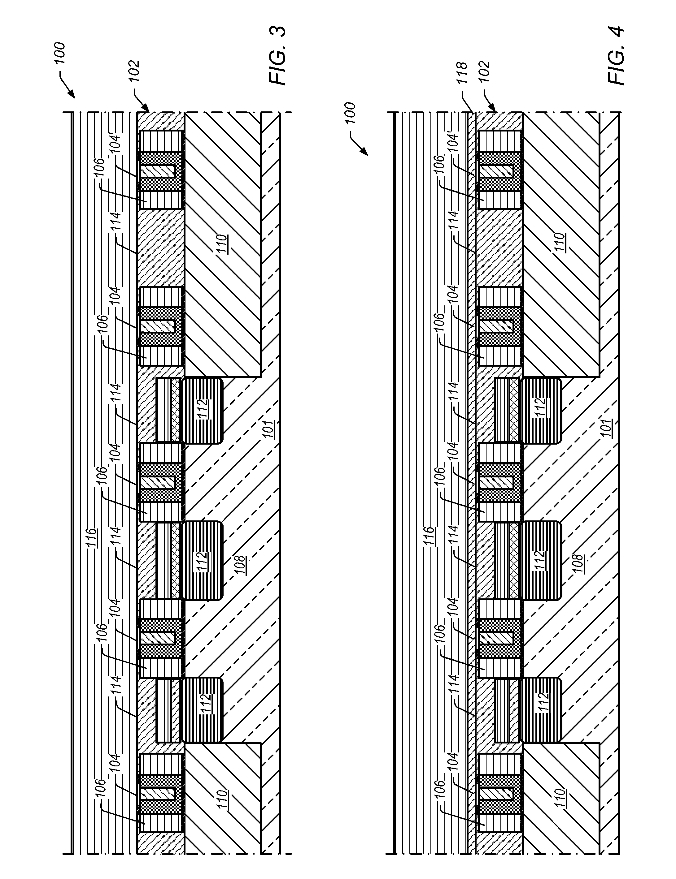
[0013]In certain embodiments, a semiconductor device fabrication process includes providing a transistor comprising a plurality of replacement metal gates on a semiconductor substrate with first gates having sources and drains and at least one second gate being isolated from the first gates. The transistor includes gate spacers of a first insulating material around each gate and a first insulating layer of a second insulating material between the gates and gate spacers. At least some of the second insulating material overlies sources and drains of the first gates.

[0014]One or more insulating mandrels are formed and aligned over the gates. The insulating mandrels include the first insulating material. Mandrel spacers are formed around each insulating mandrel. The mandrel spacers include the first insulating material. A second insulating layer of the second insulating material is formed over the transistor.

[0015]One or more first trenches to the sources and drains of the first gates a...


PUM


Abstract

A semiconductor device fabrication process includes forming insulating mandrels over replacement metal gates on a semiconductor substrate with first gates having sources and drains and at least one second gate being isolated from the first gates. Mandrel spacers are formed around each insulating mandrel. The mandrels and mandrel spacers include the first insulating material. A second insulating layer of the second insulating material is formed over the transistor. One or more first trenches are formed to the sources and drains of the first gates by removing the second insulating material between the insulating mandrels. A second trench is formed to the second gate by removing portions of the first and second insulating materials above the second gate. The first trenches and the second trench are filled with conductive material to form first contacts to the sources and drains of the first gates and a second contact to the second gate.

Description

BACKGROUND OF THE INVENTION[0001]1. Field of the Invention[0002]This invention relates generally to semiconductor processes for forming transistors and, more specifically, to processes for forming trench contacts and local interconnects to a replacement gate structure on a semiconductor substrate.[0003]2. Description of the Related Art[0004]Transistors such as planar transistors have been the core of integrated circuits for several decades. The size of the individual transistors has steadily decreased through advances in process development and the need to increase feature density. Current scaling employs 32 nm technologies with development also progressing towards 20 nm and beyond technologies (e.g., 15 nm technologies).[0005]Replacement gate processes (flows) are becoming more commonly utilized as they avoid certain problems found in gate first processes. For example, replacement gate processes may avoid problems associated with the stability of the work function material used in ...

Claims


Application Information

Patent Timeline
Patent Type & Authority Applications(United States)
IPC IPC(8): H01L29/78H01L21/768
CPCH01L21/76895H01L27/088H01L21/76801H01L21/76897H01L29/7809H01L29/7812H01L29/7813
Inventor SCHULTZ, RICHARD T.
Owner ADVANCED MICRO DEVICES INC
Why Eureka
Try Eureka