Image processing device, imaging device, and image processing method

a technology of image processing and imaging device, applied in image enhancement, color signal processing circuit, instruments, etc., can solve the problems of affecting the captured image, unnecessary light can be larger compared to the optical system, and achieve the effect of appropriate reduction

Active Publication Date: 2013-05-16
PANASONIC CORP
View PDF8 Cites 14 Cited by
  • Summary
  • Abstract
  • Description
  • Claims
  • Application Information

AI Technical Summary

Benefits of technology

[0014]According to the present invention, an unnecessary light component included in a captured image can be appropriately reduced by image processing, even when luminance is saturated in the image captured through an optical system including a diffractive optical element.

Problems solved by technology

When an image of a bright object is captured by an imaging device that captures an object, unnecessary light around the object can be bright enough and visible, adversely affecting the captured image.
Especially when a diffractive lens having a diffraction grating is used, unnecessary light due to unnecessary order diffracted light other than the design order of a diffractive lens is generated, and thus the unnecessary light can be larger compared to the optical system including only an aspheric lens.

Method used


Image

  • Image processing device, imaging device, and image processing method
  • Image processing device, imaging device, and image processing method
  • Image processing device, imaging device, and image processing method

Examples


embodiment 1

[0086]The following describes Embodiment 1 of the present invention with reference to the drawings.

[0087]FIG. 9 is a block diagram showing a functional structure of an imaging device according to Embodiment 1 of the present invention. The imaging device according to this embodiment includes an imaging unit 1 and an image processing device 2.

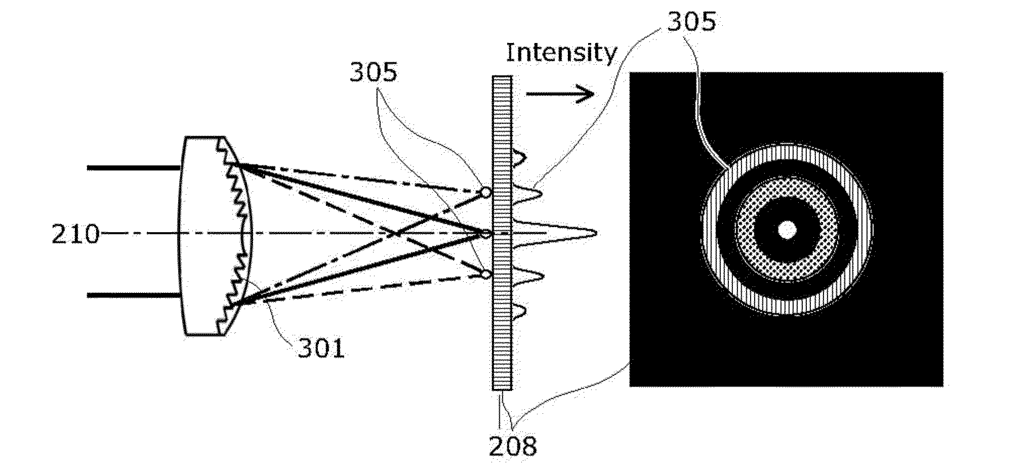
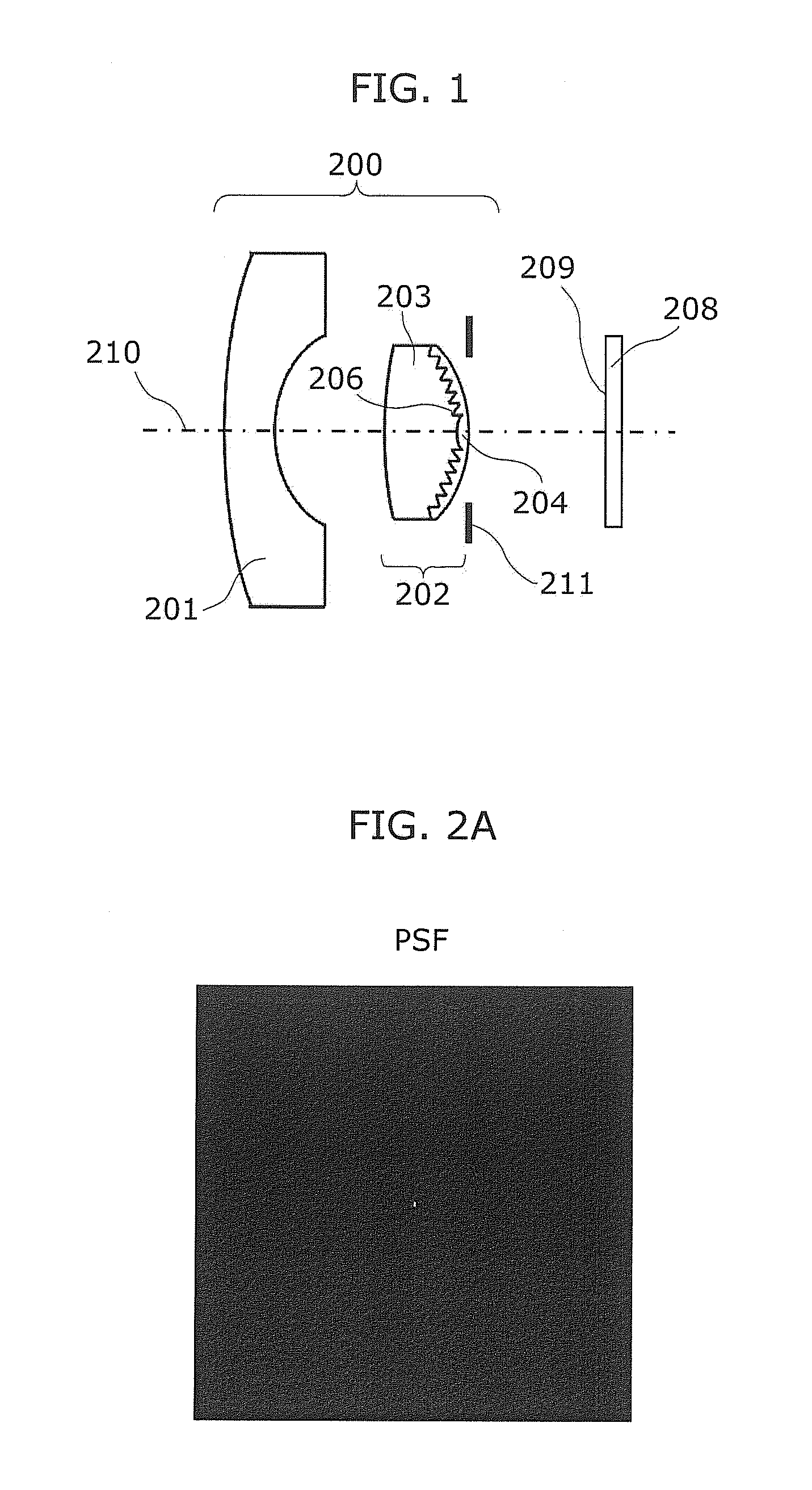
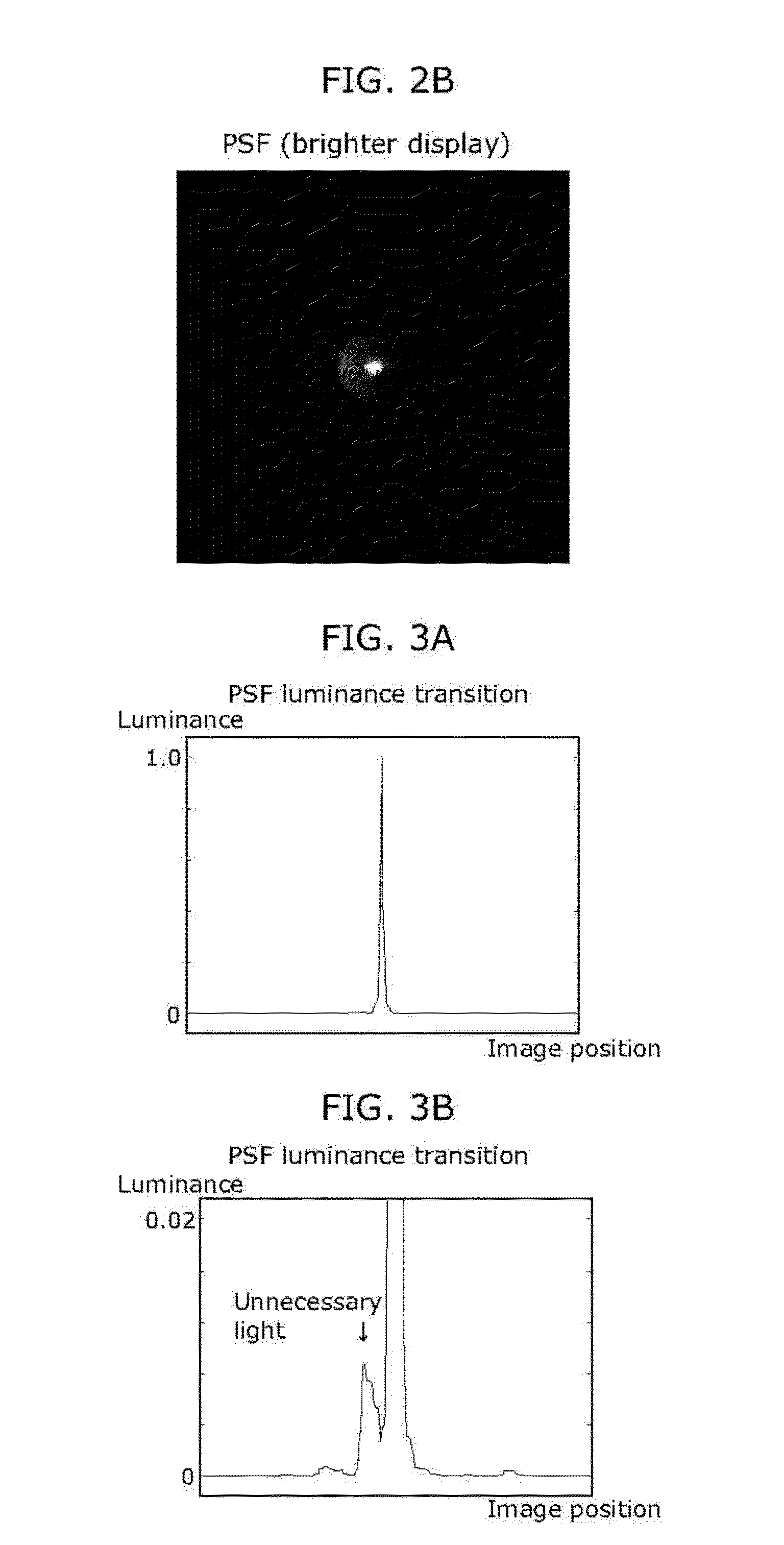
[0088]The imaging unit 1 produces a captured image Ir(x, y) by capturing, in an imaging device such as a CCD or a CMOS, an object image through an optical system including a diffractive optical element. Represented by “x” and “y” are a position in the vertical direction and the horizontal direction, respectively, in an image.

[0089]The image processing device 2 reduces an unnecessary light component in an image captured through the optical system including the diffractive optical element. Note that the unnecessary light component is the luminance of the image formed by unnecessary light (unnecessary light image).

[0090]As shown in FIG. 9, the image...

embodiment 2

[0144]The following describes Embodiment 2 of the present invention with reference to the drawings. The structure of an imaging device according to this embodiment is identical to the structure shown in FIG. 9. However, in this embodiment, the processing performed by the flare position setting unit 12 and the flare model luminance adjustment unit 13 is different from the processing performed according to Embodiment 1. Thus, the following describes mainly the processing performed by the flare position setting unit 12 and the flare model luminance adjustment unit 13. Other processing is the same as the processing performed according to Embodiment 1 and thus the detailed descriptions thereof are omitted.

[0145]Each of FIG. 22A and FIG. 22B show captured image Ir(x, y) used in this embodiment. The captured images shown in FIG. 22A and FIG. 22B are simulated images that are produced based on the PSF shown in FIG. 2A and objects shown in FIG. 15A and FIG. 15B. FIG. 22A shows the captured i...


PUM


Abstract

An image processing device includes: a luminance saturation position detection unit which detects a luminance saturation position to produce a light source image; a flare model production unit which produces a flare model image based on the light source image and optical characteristics data of the optical system; a flare position setting unit which sets, as a flare position, a predetermined image position in the captured image and located near the luminance saturation position and on a side of an optical axis relative to the luminance saturation position; a flare model luminance adjustment unit which produces the estimated flare image by adjusting luminance gain of the flare model image, based on a relationship between a luminance value of the captured image at the flare position and a luminance value of the flare model image at the flare position; and an unnecessary light subtraction unit which subtracts the estimated flare image from the captured image.

Description

TECHNICAL FIELD[0001]The present invention relates to techniques for reducing an unnecessary light component in an image captured through an optical system including a diffractive optical element by performing image processing.BACKGROUND ART[0002]When an image of a bright object is captured by an imaging device that captures an object, unnecessary light around the object can be bright enough and visible, adversely affecting the captured image. Especially when a diffractive lens having a diffraction grating is used, unnecessary light due to unnecessary order diffracted light other than the design order of a diffractive lens is generated, and thus the unnecessary light can be larger compared to the optical system including only an aspheric lens.[0003]There is a conventional technique which reduces the unnecessary light by performing image processing. For example, according to PTL 1, unnecessary light is estimated based on a convolution integral of a point spread function (PSF) of an u...

Claims


Application Information

Patent Timeline
Patent Type & Authority Applications(United States)
IPC IPC(8): H04N5/235
CPCH04N5/3572H04N5/2351G06T2207/20224G06T5/10G06T2207/20056G06T5/003H04N25/615H04N25/61H04N23/71
Inventor OYAMA, ICHIRO
Owner PANASONIC CORP
Why Eureka
Try Eureka