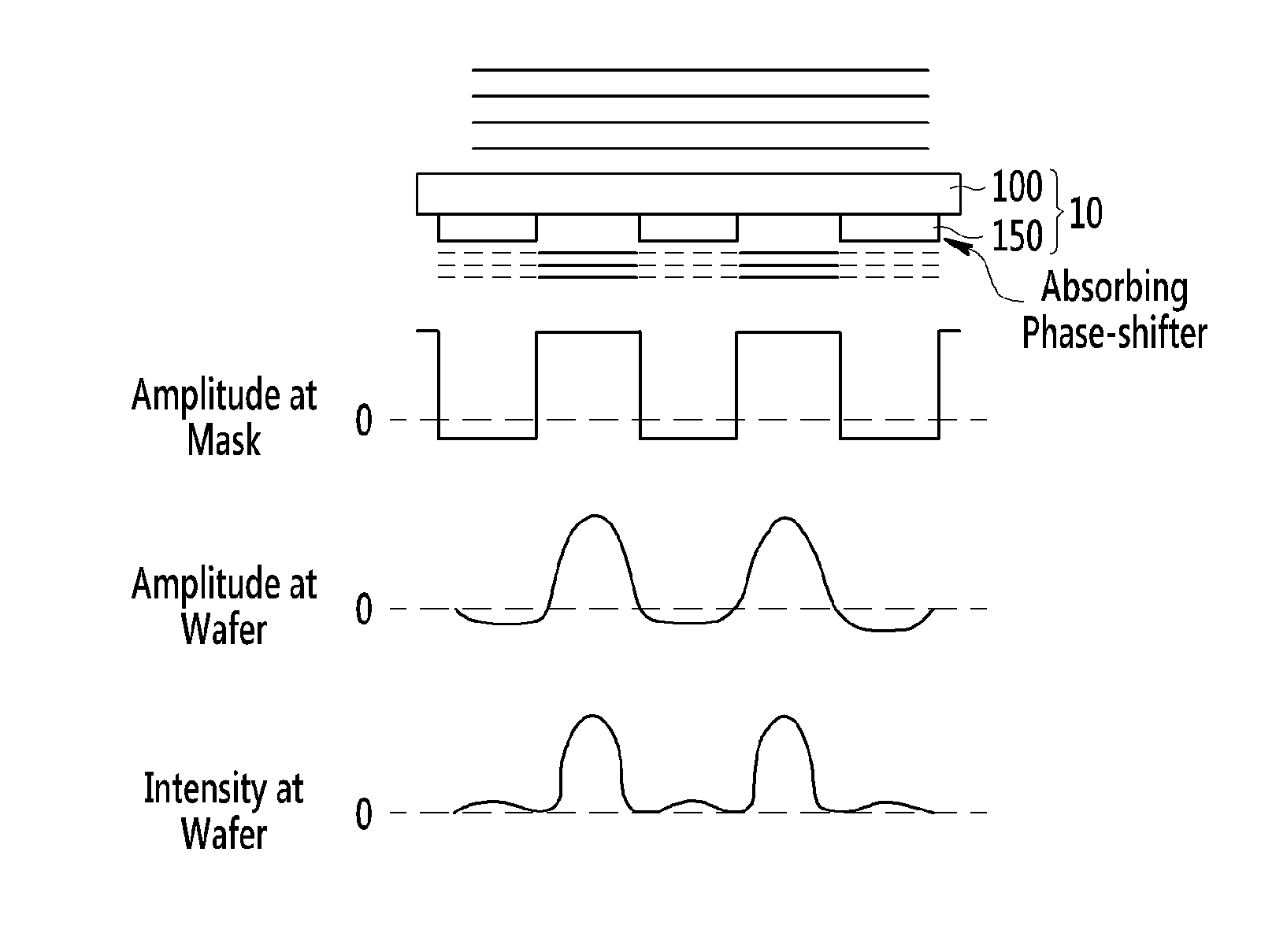
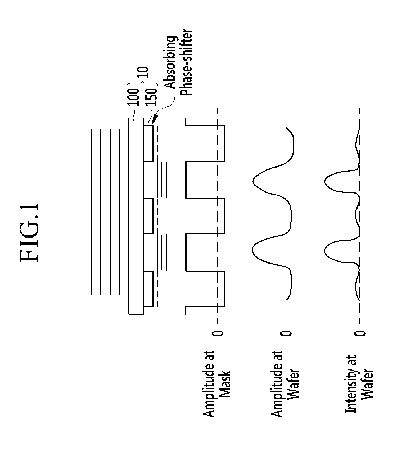
Mask for exposure and method of fabricating substrate using said mask

a mask and substrate technology, applied in the field of masks for exposure and substrate fabrication, can solve the problems of limited resolution, significant time and cost, and the flat panel display field has not seen much demand for fine patterns or improved fine pattern formation techniques, etc., to achieve the effect of improving the quality of the display device, reducing cost, and relatively small defect ratio

Active Publication Date: 2013-05-16
SAMSUNG DISPLAY CO LTD
View PDF4 Cites 11 Cited by
  • Summary
  • Abstract
  • Description
  • Claims
  • Application Information

AI Technical Summary

Benefits of technology

[0031]According to the exemplary embodiments of the present invention, a fine pattern beyond, or formed finer than, a critical resolution of the exposer can be formed without replacing or changing the exposer, thereby making it possible to reduce cost. Further, the resulting defect ratio is also relatively small, thereby making it possible to improve quality of the display device.
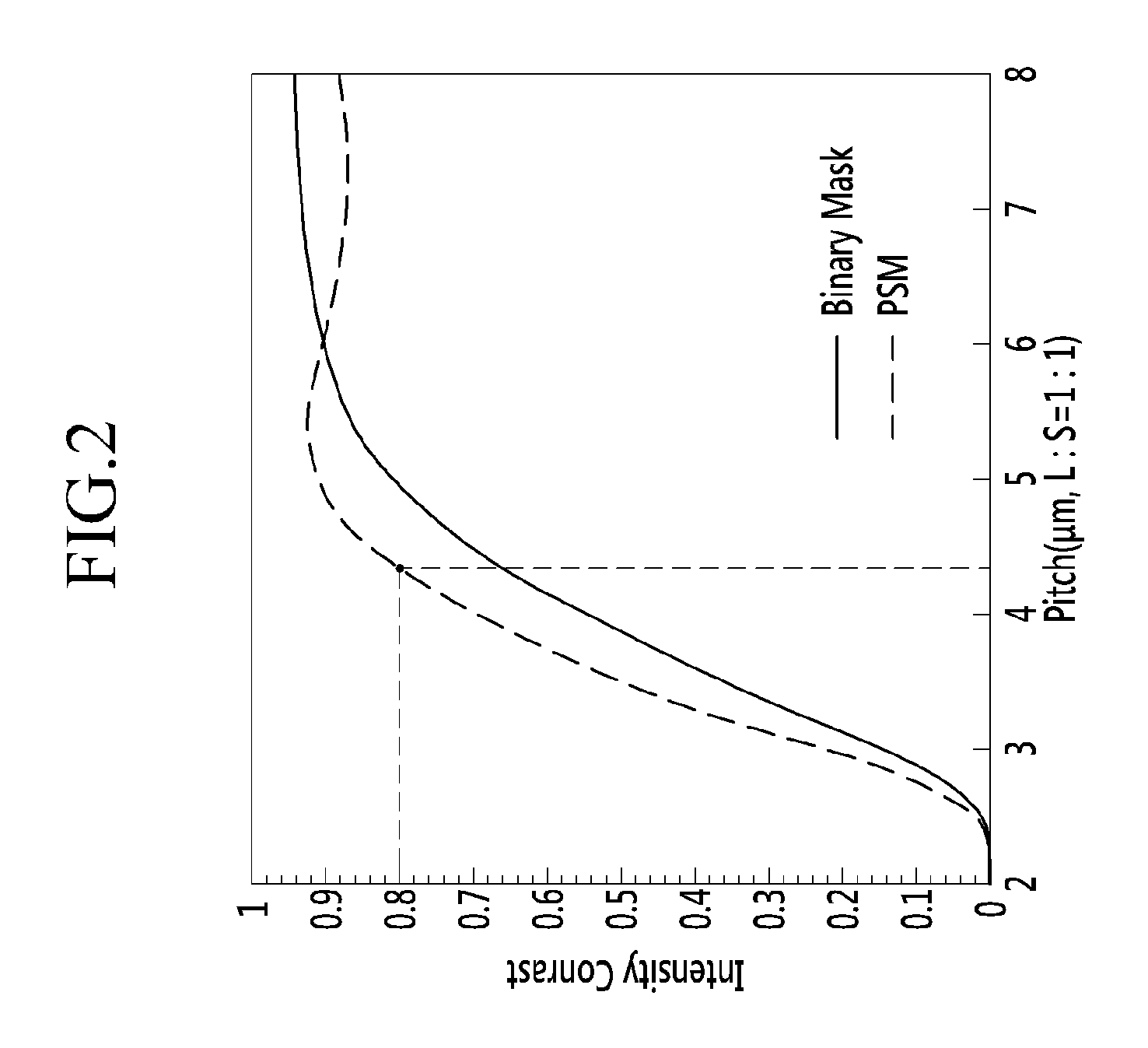
[0032]As described above, it is possible to form a pattern having a pitch smaller than the critical resolution provided in the exposer by using a characteristic of the phase shift layer of invention photolithography mask. The fine pattern can thus be formed, thereby making it possible to improve an aperture ratio and display quality of the display device. In addition, since only the phase shift layer is formed on the mask, the phase shift layer can be formed on the substrate using conventional equipment and processes, thereby making it possible to manufacture the mask at low cost and with less difficulty.

Problems solved by technology

Unlike the general semiconductor field, the flat panel display field has not seen much demand for fine patterns, or improved fine pattern formation techniques.
However, in the drive for increased resolution of these display devices, pixel sizes have shrunk to below the critical resolution of current exposers, thus spawning a demand for fine pattern formation.
Previously, the exposer used for manufacturing the display device used a complex wavelength light source having a plurality of light sources, but this limited resolution.
However, the method requires remodeling of the exposer and introduction of new equipment, which entails significant time and cost.
Further, since the change to a single wavelength light source and the increase in the NA value reduce the critical resolution and a depth of focus, non-uniformity defects can occur in a display device field using a large-area substrate.
In this case, since the fine pattern is formed beyond the critical resolution of the exposer, many defects occur in the formed fine pattern, such that yield reduction and defect frequency become issues.

Method used


Image

  • Mask for exposure and method of fabricating substrate using said mask
  • Mask for exposure and method of fabricating substrate using said mask
  • Mask for exposure and method of fabricating substrate using said mask

Examples


Embodiment Construction

[0041]The present invention will be described more fully hereinafter with reference to the accompanying drawings, in which exemplary embodiments of the invention are shown. As those skilled in the art would realize, the described embodiments may be modified in various different ways, all without departing from the spirit or scope of the present invention.

[0042]In the drawings, the thickness of layers, films, panels, regions, etc., are exaggerated for clarity. Like reference numerals designate like elements throughout the specification. It will be understood that when an element such as a layer, film, region, or substrate is referred to as being “on” another element, it may be directly on the other element or intervening elements may also be present. In contrast, when an element is referred to as being “directly on” another element, there are no intervening elements present.

[0043]Hereinafter, a mask for exposure according to an exemplary embodiment of the present invention will be de...


PUM

PropertyMeasurementUnit
transmittanceaaaaaaaaaa

Abstract

Provided is a photolithography mask capable of forming fine patterns beyond a critical resolution of an exposer without replacing or changing the exposer. The mask includes an at least partially light absorbing phase shift layer and uses a complex wavelength light source.

Description

CROSS-REFERENCE TO RELATED APPLICATION[0001]This application claims priority to, and the benefit of, Korean Patent Application No. 10-2011-0119567 filed in the Korean Intellectual Property Office on Nov. 16, 2011, the entire contents of which are incorporated herein by reference.BACKGROUND OF THE INVENTION[0002](a) Field of the Invention[0003]Embodiments of the present invention relate generally to flat panel display fabrication. More specifically, embodiments of the present invention relate to a mask for exposure during a flat panel display fabrication process, and a method of fabricating a substrate using the mask.[0004](b) Description of the Related Art[0005]Today, flat panel display devices are fabricated in various ways. The flat panel display devices can include various display devices such as a liquid crystal display, an organic light emitting device, an electrophoretic display, an MEMS display device, and a 3D display device.[0006]In each of these devices, there exists a gro...

Claims


Application Information

Patent Timeline
Patent Type & Authority Applications(United States)
IPC IPC(8): G03F7/20G03F1/26
CPCG03F1/32G03F1/00G03F1/26
Inventor KIM, BONG-YEONKANG, MINLEE, JONG KWANGJU, JIN HO
Owner SAMSUNG DISPLAY CO LTD
Why Eureka
Try Eureka