Method for fabricating ultra-fine nanowire

a nanowire and ultra-fine technology, applied in the field of manufacturing transistors, can solve the problems of limiting the application of electron beam lithography in mass manufacturing, high cost, and low efficiency, and achieve the effects of reducing the width of nanowires, and reducing the cost of manufacturing

Inactive Publication Date: 2013-05-23
PEKING UNIV
View PDF6 Cites 1 Cited by
  • Summary
  • Abstract
  • Description
  • Claims
  • Application Information

AI Technical Summary

Benefits of technology

[0022]A technical advantage and effect of the embodiment of invention is as follows.
[0023]In a fabricating process of integrated circuit, since an integrated degree is getting higher and higher, a width of a nanowire pattern is required to be smaller and smaller, and meanwhile an industry cost is desirable to be reduced. If the fine nanowire is fabricated by using an electron beam lithography and an etching process, the cost is substantially high, which is not advantageous in a industry manufacturing. Further, if the nanowire is oxidized though an oxidation approach in order to reduce the width of the nanowire, it is certain to extend a reaction time, thus limiting the manufacturing and application for industry production. In the present invention, a process method for fabricating an ultra-thin nanowire by a combination of performing a trimming process on a mask to reduce a width of the mask and blocking an oxidation through the mask is provided. By initially performing a trimming process on the mask, the width of the mask is reduced, and meanwhile only an top portion of a primary nanowire is blocked from being oxidized. Moreover, by further performing a wet oxidation process, sides and a part of the top portion of the nanowire are oxidized at the same time, while other part of the top portion is blocked from being oxidized by the mask, and thus the width of the nanowire is considerably reduced. A diameter of the floated ultra-thin nanowire fabricated by the method can be controlled to 20 nm below by a thickness of a deposited silicon oxide film, a width of the silicon oxide nanowire after trimming, and a time and a temperature for performing a wet oxidation process. Also, since a speed of the wet oxidation process is faster, the width of the nanowire obtained by a conventional photolithography is reduced faster. Moreover, when fabricating an ultra-thin nanowire by using the method, the cost is reduced and it is more feasible to be implemented.

Problems solved by technology

However, some drawbacks, such as a low efficiency and a high cost, are existed as well, thus limiting the application of the electron beam lithography in a mass manufacturing.
Further, during the electron beam lithography, an electron scattering may occur, which leads to a proximity effect and causes a huge challenge when fabricating a nanowire smaller than 20 nm.

Method used


Image

  • Method for fabricating ultra-fine nanowire
  • Method for fabricating ultra-fine nanowire
  • Method for fabricating ultra-fine nanowire

Examples


Embodiment Construction

[0027]A detailed description of the invention will be described with reference to the accompany drawings and an embodiment.

[0028]An ultra-fine nanowire with a diameter of about 20 nm may be fabricated by the following steps.

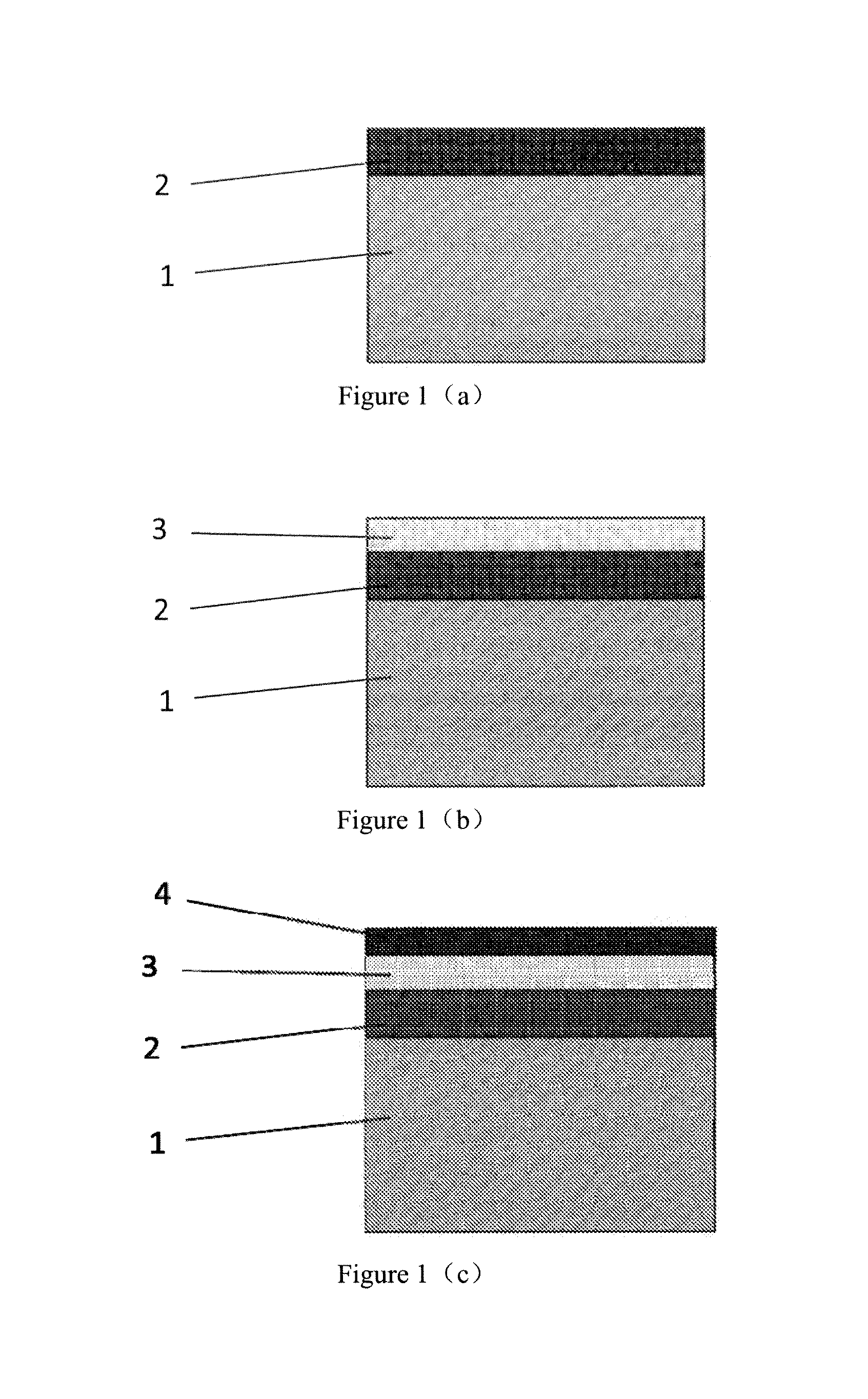
[0029]1. A silicon oxide film with a thickness of 1500 Å is deposited on a silicon substrate through a low pressure chemical vapor deposition process, as shown in FIG. 1(a).

[0030]2. A silicon nitride film with a thickness of 500 Å is deposited through a low pressure chemical vapor deposition process, as shown in FIG. 1(b).

[0031]3. A photoresist is coated on the silicon nitride film, as shown in FIG. 1(c).

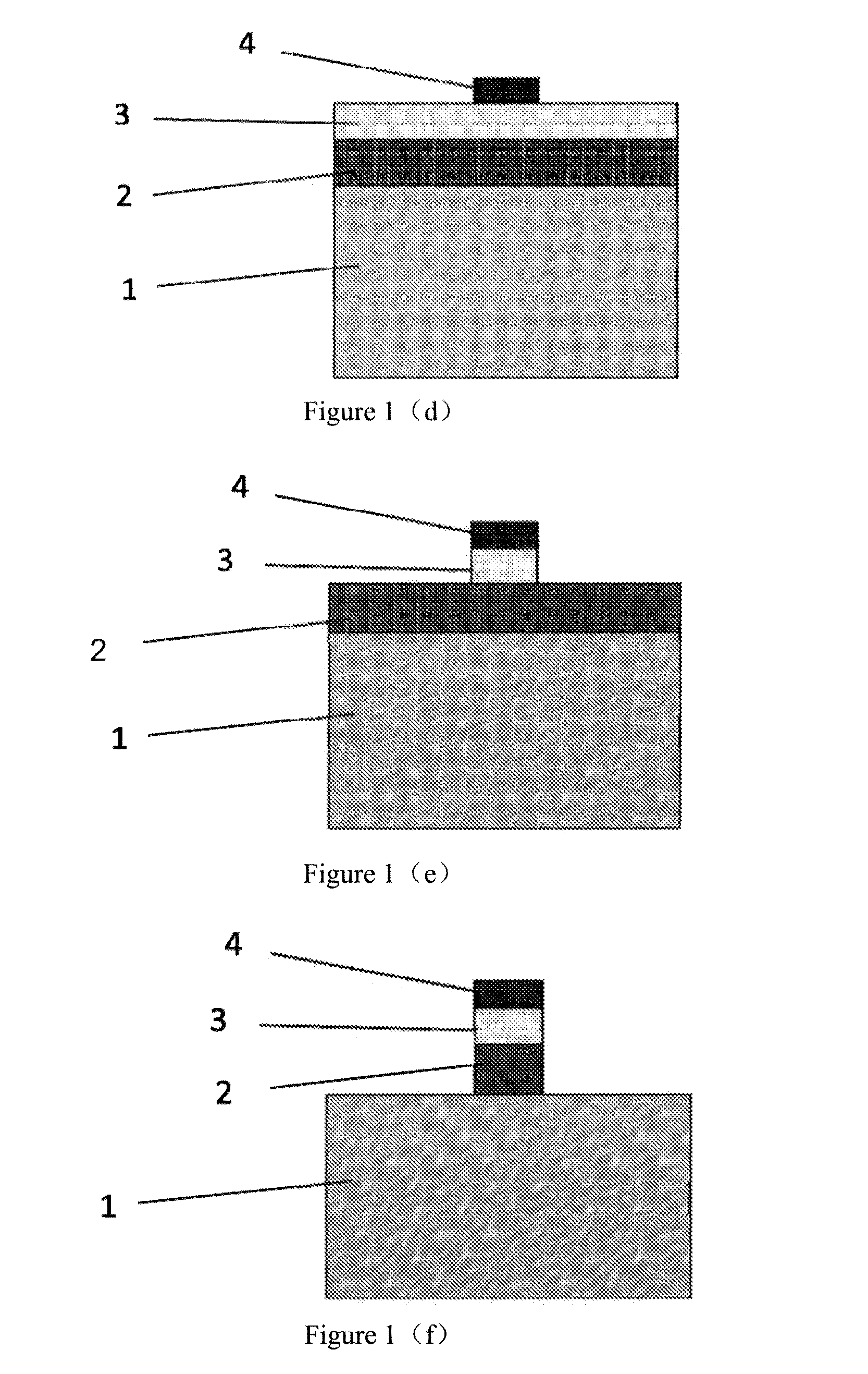
[0032]4. A region where a hard mask for the silicon nanowire is to be formed is defined through a photolithography process, as shown in FIG. 1(d).

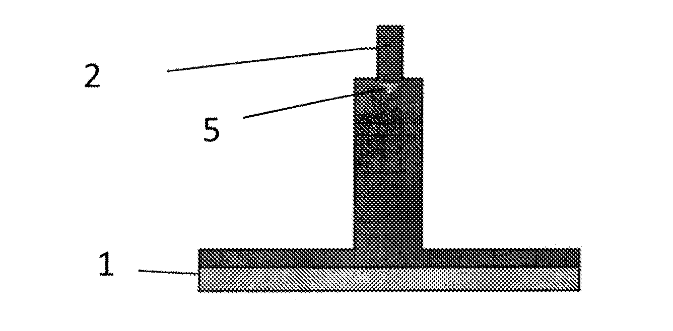
[0033]5. The silicon nitride film is etched by 500 Å through an anisotropic dry etching process, so as to transfer a pattern of the photoresist onto the silicon nitride film, as shown in FIG. 1(e).

[0034]6. The silicon o...


PUM

PropertyMeasurementUnit
thicknessaaaaaaaaaa
diameteraaaaaaaaaa
volume ratioaaaaaaaaaa

Abstract

Disclosed herein is a method for fabricating an ultra-fine nanowire by combining a trimming process and a mask blocking oxidation process. The ultra-thin nanowire is fabricated by a combination of performing a trimming process on a mask to reduce a width of the mask and blocking an oxidation through the mask. A diameter of the floated ultra-thin nanowire fabricated by the method is controlled to 20 nm below by a thickness of a deposited silicon oxide film, a width of the silicon oxide nanowire after trimming, and a time and a temperature for performing a wet oxidation process. Also, since a speed of the wet oxidation process is faster, the width of the nanowire obtained by a conventional photolithography is reduced faster. Moreover, when fabricating an ultra-thin nanowire by using the method, the cost is reduced and it is more feasible to be implemented.

Description

CROSS-REFERENCES TO RELATED APPLICATION[0001]The present application claims priority to Chinese Patent Application No. 201110375066.5, filed on Nov. 23, 2011, which is incorporated herein by reference in its entirety.FIELD OF THE INVENTION[0002]An embodiment of the prevent invention relates to a field of manufacturing a transistor in a microelectronic semiconductor device, and more particularly, relates to a method for fabricating an ultra-fine nanowire by combining a trimming process and a mask blocking oxidation process.BACKGROUND OF THE INVENTION[0003]With the development of integrated circuit industry, a higher integration degree is demanded more and more, and a feature size of a field effect transistor is required to be scaled down accordingly. At the same time, it is desirable to obtain a better performance and a lower manufacturing cost. In manufacturing, there has been a stricter requirement for a photolithography process. Electron beam lithography is widely used at present ...

Claims


Application Information

Patent Timeline
Patent Type & Authority Applications(United States)
IPC IPC(8): H01L21/308B82Y40/00
CPCH01L29/0665H01L29/0673B82Y10/00B82Y30/00B82Y40/00
Inventor HUANG, RUSUN, SHUAIAI, YUJIEFAN, JIEWENWANG, RUNSHENGXU, XIAOYAN
Owner PEKING UNIV
Why Eureka
Try Eureka