Semiconductor integrated circuit and optical sensor device using the same
a technology of semiconductor integrated circuit and optical sensor, which is applied in the direction of photometry using electric radiation detectors, electron multiplier details, instruments, etc., can solve the problems of reducing affecting so as to reduce the number of fuses to be melted and cut, the effect of preventing adverse effects on the quality of semiconductor integrated circuit, and suppressing adverse effects on the quality of semiconductor
- Summary
- Abstract
- Description
- Claims
- Application Information
AI Technical Summary
Benefits of technology
Problems solved by technology
Method used
Image
Examples
first embodiment
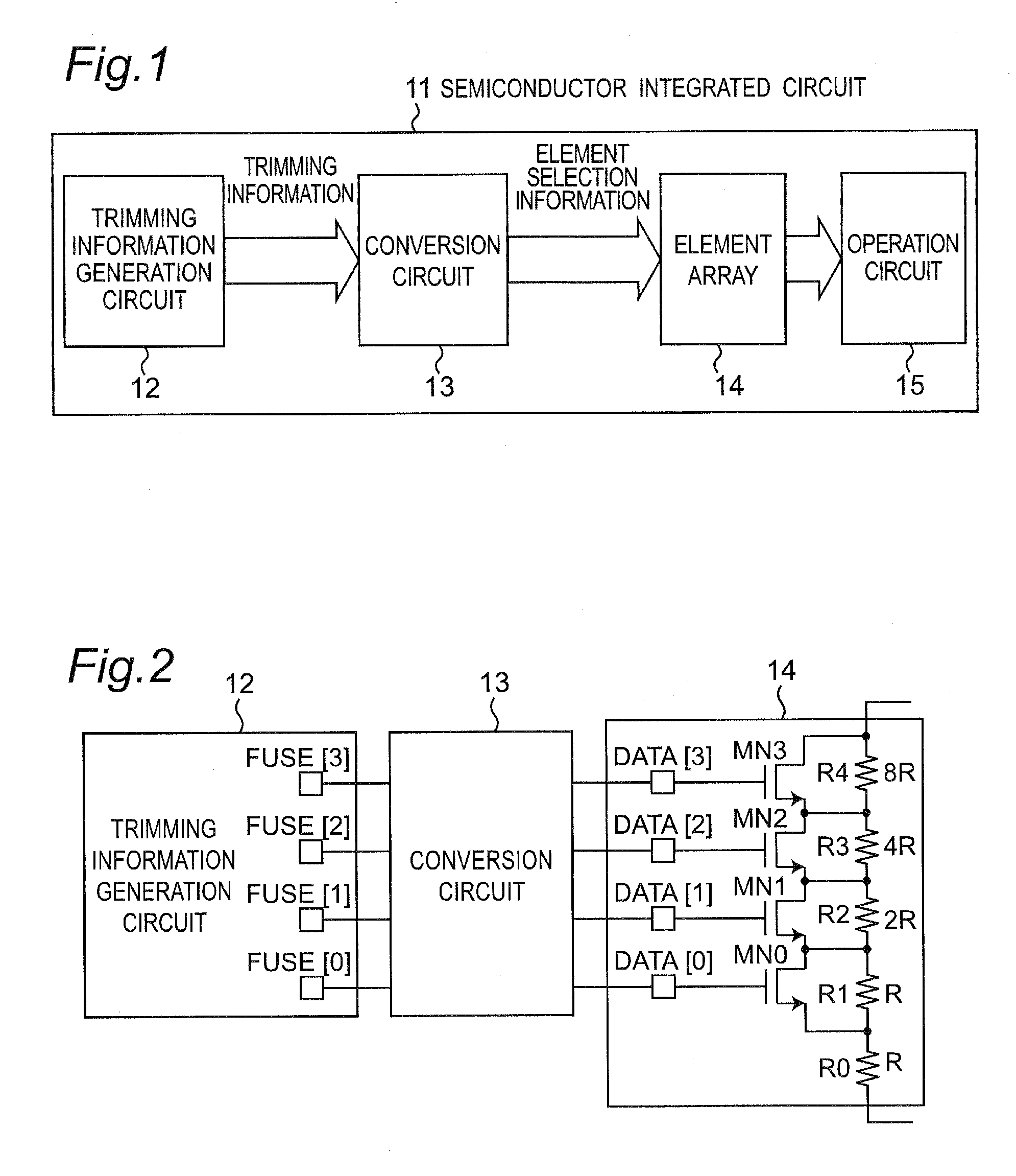
[0090]FIG. 1 is an outlined block diagram of a semiconductor integrated circuit according to this embodiment.
[0091]In FIG. 1, reference sign 11 denotes a semiconductor integrated circuit, which includes a trimming information generation circuit 12, a conversion circuit 13, an element array 14, and an operation circuit 15.
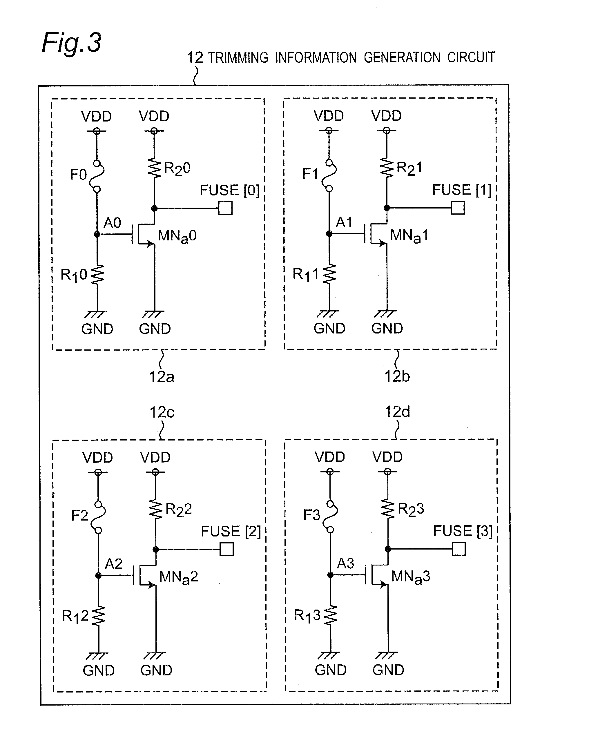
[0092]In this configuration, the trimming information generation circuit 12, having a plurality of fuses contained therein as will be detailed later, generates trimming signals representing whether or not the individual fuses have been melted and cut by trimming, and outputs trimming information formed of a bit string representing trimming signals for all the fuses.
[0093]The conversion circuit 13 performs conversion, as will be detailed later, of a bit string of trimming information outputted from the trimming information generation circuit 12 to generate element selection information formed of a bit string. According to the element selection information generated b...
second embodiment
[0138]In the first embodiment, as described above, correspondence between the combined resistance values of resistors R shown in FIG. 5C and the trimming information shown in FIG. 5A is fulfilled by setting the array of trimming information corresponding to the combined resistance values ‘16R’ to ‘9R’ into a descending order from ‘15’ to ‘8’ in decimal number. Meanwhile, the array of trimming information corresponding to the combined resistance values ‘8R’ to ‘1R’ is set into an ascending order from ‘0’ to ‘7’ in decimal number.
[0139]In this case, as can be seen from FIG. 5D, the number of melted-and-cut fuses does not simply increase in response to increases in deviation from ‘0’ fuses corresponding to the mean value in the appearance frequency distribution shown in FIG. 5E. The number of melted-and-cut fuses once decreases as from ‘3’ to ‘2’ fuses in the minus side of deviation and as from ‘2’ to ‘1’ fuses in the plus side of deviation.
[0140]From a viewpoint of lessening the numbe...
PUM
 Abstract
Description
Claims
Application Information
 - R&D
- Intellectual Property
- Life Sciences
- Materials
- Tech Scout
- Unparalleled Data Quality
- Higher Quality Content
- 60% Fewer Hallucinations
Browse by: Latest US Patents, China's latest patents, Technical Efficacy Thesaurus, Application Domain, Technology Topic, Popular Technical Reports.
© 2025 PatSnap. All rights reserved.Legal|Privacy policy|Modern Slavery Act Transparency Statement|Sitemap|About US| Contact US: help@patsnap.com


