Complex primary optics and methods of fabrication

a technology of primary optics and fabrication methods, applied in the direction of manufacturing tools, applications, instruments, etc., can solve the problems of insufficient process efficiency, loss of light emitted by led chips, and inability to meet the requirements of many applications,

Active Publication Date: 2013-05-30
CREELED INC
View PDF4 Cites 58 Cited by
  • Summary
  • Abstract
  • Description
  • Claims
  • Application Information

AI Technical Summary

Benefits of technology

[0017]The present invention provides various embodiments of optics and methods of fabricating the same such that these optics are capable of beam shaping and can be manufactured in batches or arrays. Furthermore, these optics may include overhangs or tapered shapes without the need for complex molds with moving parts.

Problems solved by technology

This confined emission is not generally suitable for many applications such as those requiring specific beam shaping; for example, collimated beam profiles, dispersed beam profiles, or specialized beam profiles.
This arrangement can result in some of the light emitted by the LED chip being lost due to loss mechanisms such as total internal reflection.
This reflection process is not 100% efficient, resulting in additional loss of light.
Also, reflections from these surfaces effectively create a larger, more complex light source (compared, for example, to the chip alone) which can require more complex secondary optics that can result in additional light loss.
If the diameter of the hemispherical optic is not large compared to the largest dimension of the associated LED source, the package may suffer from output losses caused by total internal reflection (“TIR”) within the optic, resulting in a low package extraction efficiency.
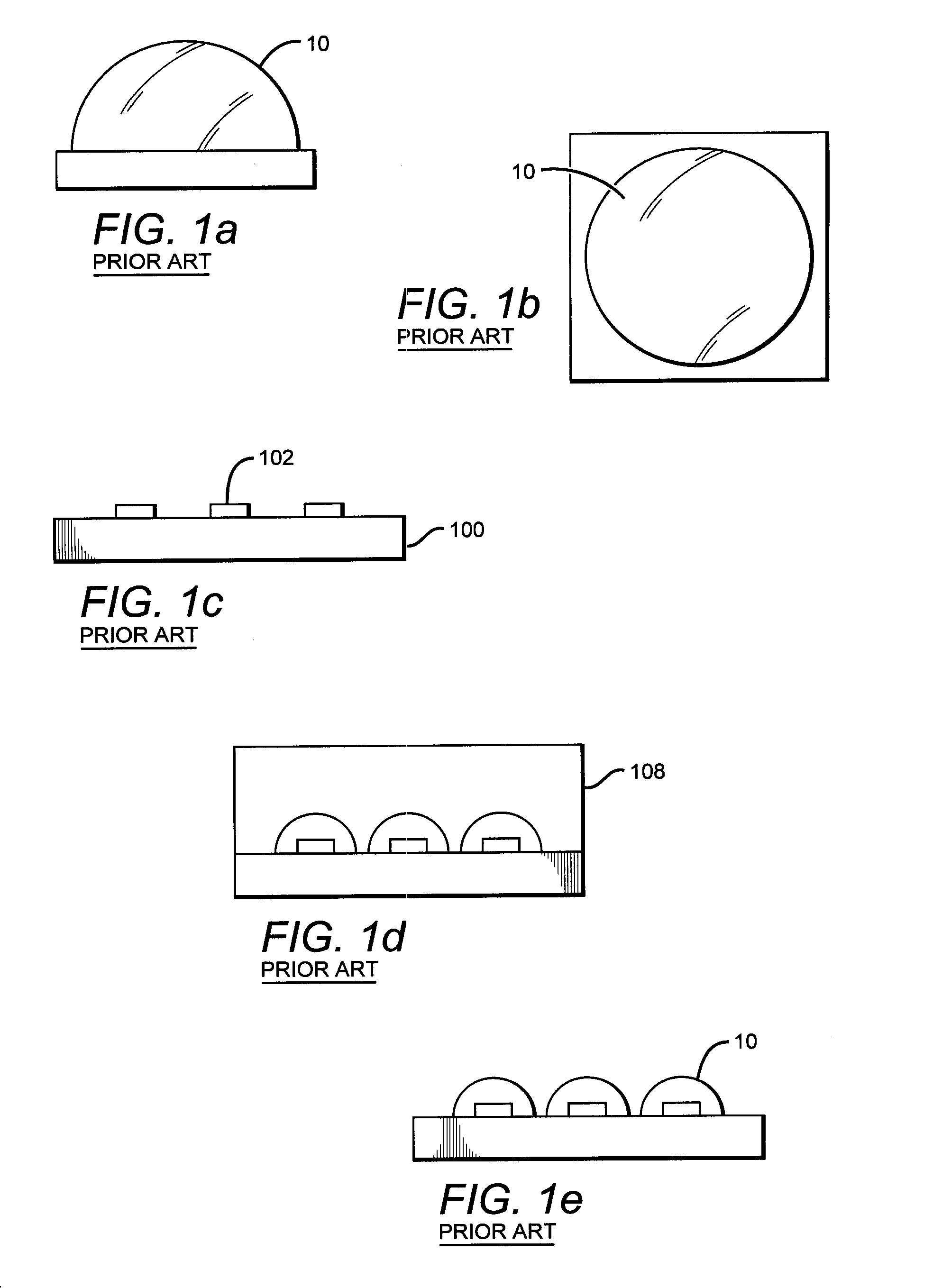
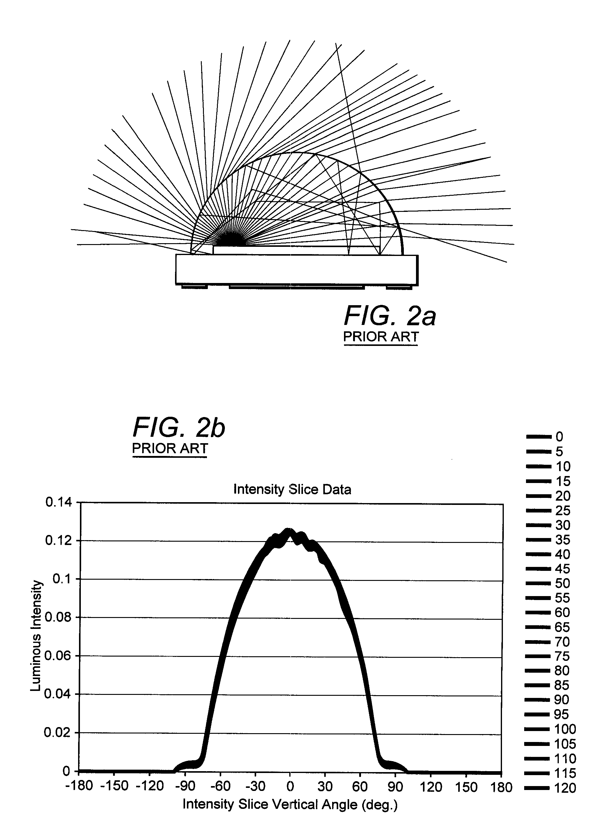
While the hemispherical optic 10 geometry is desirable with respect to efficiency and ease of fabrication, this geometry typically does little to modify the initial optical output beam profile from the LED source.
However, many such geometries are not readily fabricated by molding processes.
Specifically, since the mold cavity must be removed from the substrate surface following curing of the molded optic, it is not generally possible to mold parts which have ‘overhangs’, are tapered, or are narrower at the base (near the substrate) than at the top.
This limitation in particular can inhibit the molding of many collimating-type optics.
While there are molding techniques which can allow such geometries, they typically involve complex molds with moving parts which are not suitable for batch fabrication of many molded elements in an array on one surface.
These mold types, called side-action molds, are thus not well suited to the fabrication of dense arrays of optics on a substrate as the lateral motions of adjacent lenses would interfere.
While individual (rather than batch) molding of complex optics using side-action molds may be possible, molding LED package optics one-at-a-time is generally not feasible due to the associated high manufacturing cost and low throughput.
Alternative approaches to the fabrication of primary optics on LED packages are also generally not suitable for the batch formation of complex optic shapes.
However, the shape of such optics is determined primarily by dispensed mass, surface tension, and gravity, with little flexibility for forming specific non-hemispherical shapes such as those with an “undercut” feature.
Similarly, approaches utilizing a primary optic element which is molded separately and then attached to the LED package can be limited by the need to place the optic above the surface of the LEDs and associated electrical contacts and also provide stable attachment to the package.
Such an approach would suffer from cost, efficiency, and manufacturability issues compared to the more simple molding process.
Such secondary optics generally increase overall cost and reduce efficiency.
Further, the shape of the secondary optic can be limited by the size and geometry of the primary LED optic or lens—this can further reduce efficiency and limit the potential for beam shaping in some applications, particularly those involving collimation of the LED light, where it is helpful to bring the optical element as close to the light source (LED chip or chips) as possible.
The use of secondary optics can result in lighting solutions which are bulky, require additional design work and alignment, optical loss, and additional costs.
In addition, the materials commonly used in the fabrication of secondary optics (e.g., plastics, polycarbonate, PMMA or glass) can result in elements which are costly, heavy, and less stable with respect to degradation when subjected to the heat and high intensity light associated with lighting-class LED packages.
Additionally, depending on the application, there may be cases where a secondary optical element is required (e.g., if the required light beam profile necessitates an optical element which is too large to conveniently or economically fabricate as a primary optical element on a LED package).

Method used


Image

  • Complex primary optics and methods of fabrication
  • Complex primary optics and methods of fabrication
  • Complex primary optics and methods of fabrication

Examples


Embodiment Construction

[0071]Embodiments of the present invention provide improved light emitting device optics and packages and methods for fabricating the same, wherein the improvements are provided by fabricating more complex primary optics capable of shaping light beams over light emitters. The primary optics disclosed herein, and methods of fabricating the same, allow for more controlled or shaped light outputs from light emitters without the use of secondary optics. However, secondary optics may still be used in conjunction with these primary optics. Furthermore, the methods disclosed herein allow for the fabrication of arrays of optics according to the present invention in smaller areas because no moving parts or side action molds are required. Embodiments of the present invention may be used in combination with previously disclosed light extraction and optic approaches, allowing even greater flexibility in controlling the light emission pattern from LED devices. The invention may be applied to oth...


PUM

PropertyMeasurementUnit
temperatureaaaaaaaaaa
angleaaaaaaaaaa
wide angleaaaaaaaaaa

Abstract

A light emitter package with primary optic and method of fabricating the same is disclosed that comprises a light emitter disposed on a surface. The package further comprises at least one intermediate element on the surface and at least partially surrounding the light emitter. Furthermore, an encapsulant is over the light emitter forming a primary optic. The intermediate element at least partially defines the shape of the primary optic.

Description

BACKGROUND OF THE INVENTION[0001]1. Field of the Invention[0002]The present invention relates to fabricating light emitter packages and optical elements and, more specifically, to primary optics and packages for LED devices and methods of manufacturing such optics and packages.[0003]2. Description of the Related Art[0004]Light emitting diodes (LEDs) are solid state devices that convert electric energy to light, and generally comprise one or more active layers of semiconductor material sandwiched between oppositely doped layers. When a bias is applied across the doped layers, holes and electrons are injected into the active layer where they recombine to generate light. Light is emitted from the active layer and from all surfaces of the LED. The useful light is generally emitted in a hemispherical emission pattern in the direction of the LED's top surface, typically resulting in a predominantly Lambertian light emission profile. This confined emission is not generally suitable for man...

Claims


Application Information

Patent Timeline
Patent Type & Authority Applications(United States)
IPC IPC(8): H01L27/15H01L33/50B29C45/14H01L33/52
CPCH01L2224/48091B29C33/68G02B19/0028B29C45/14655B29C45/4457B29C33/52G02B19/0061B29C43/18H01L33/54H01L33/58H01L2933/005G02B19/0066H01L2924/00014B33Y80/00
Inventor TARSA, ERICKELLER, BERNDGUSCHL, PETERNEGLEY, GERALD
Owner CREELED INC
Why Eureka
Try Eureka