Circuit and system of using finfet for building programmable resistive devices

a technology of programmable resistive devices and finfets, which is applied in the field of circuits and systems of using finfets for building programmable resistive devices, can solve the problems of poor thermal conductivity of tall and narrow silicon islands erected from a substrate, and the cell size of electrical fuse using silicided polysilicon tends to be very large, so as to reduce the cost and reduce the size of the cell

Active Publication Date: 2013-06-13
ATTOPSEMI TECH CO LTD
View PDF0 Cites 153 Cited by
  • Summary
  • Abstract
  • Description
  • Claims
  • Application Information

AI Technical Summary

Benefits of technology

[0013]Embodiments of programmable resistive device cells using MOS devices or diodes in standard FinFET technologies as program selectors are disclosed. The programmable resistive devices can be fabricated using standard FinFET processes to reduce cell size and cost.

Problems solved by technology

As a result, the cell size of an electrical fuse using silicided polysilicon tends to be very large.
Other than distinct electrical properties from the planar MOS, the tall and narrow silicon islands erected from a substrate have poor thermal conductivity.

Method used


Image

  • Circuit and system of using finfet for building programmable resistive devices
  • Circuit and system of using finfet for building programmable resistive devices
  • Circuit and system of using finfet for building programmable resistive devices

Examples


Embodiment Construction

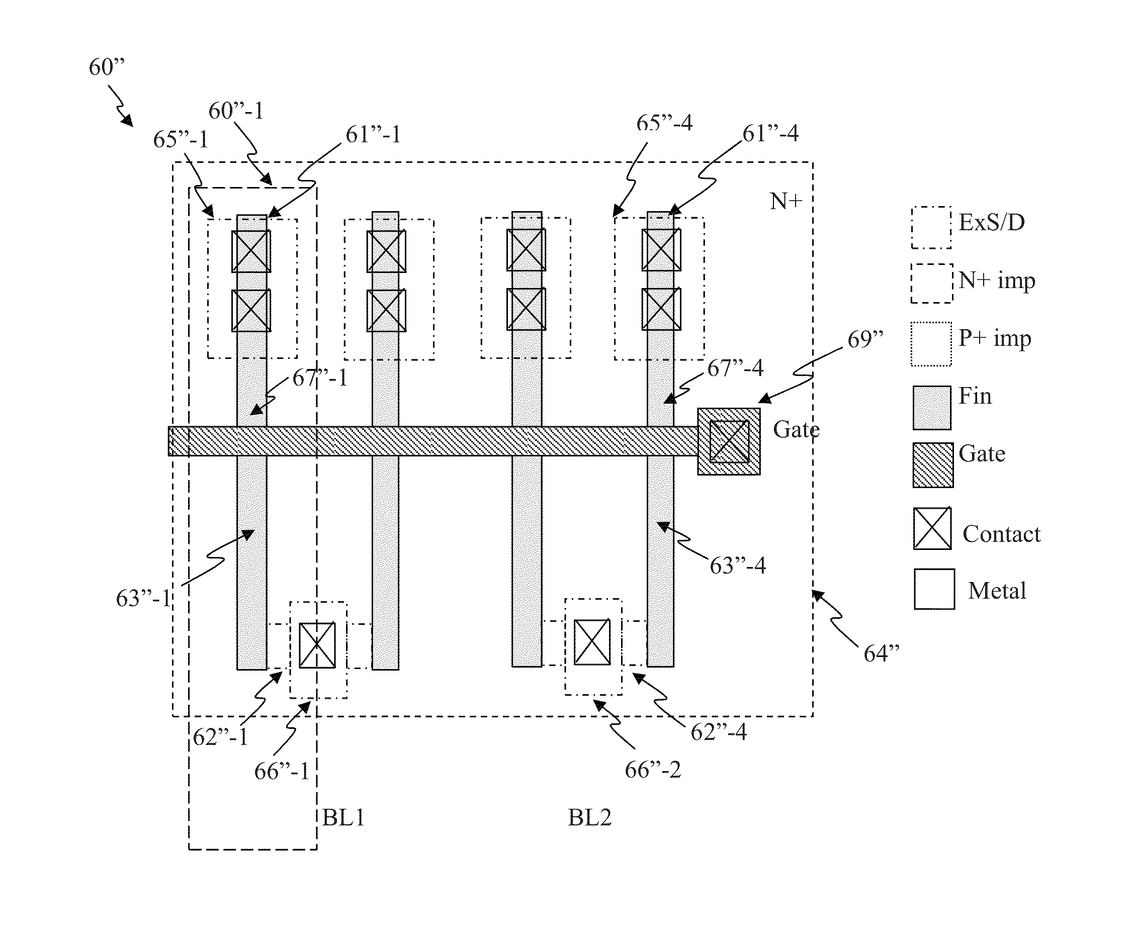
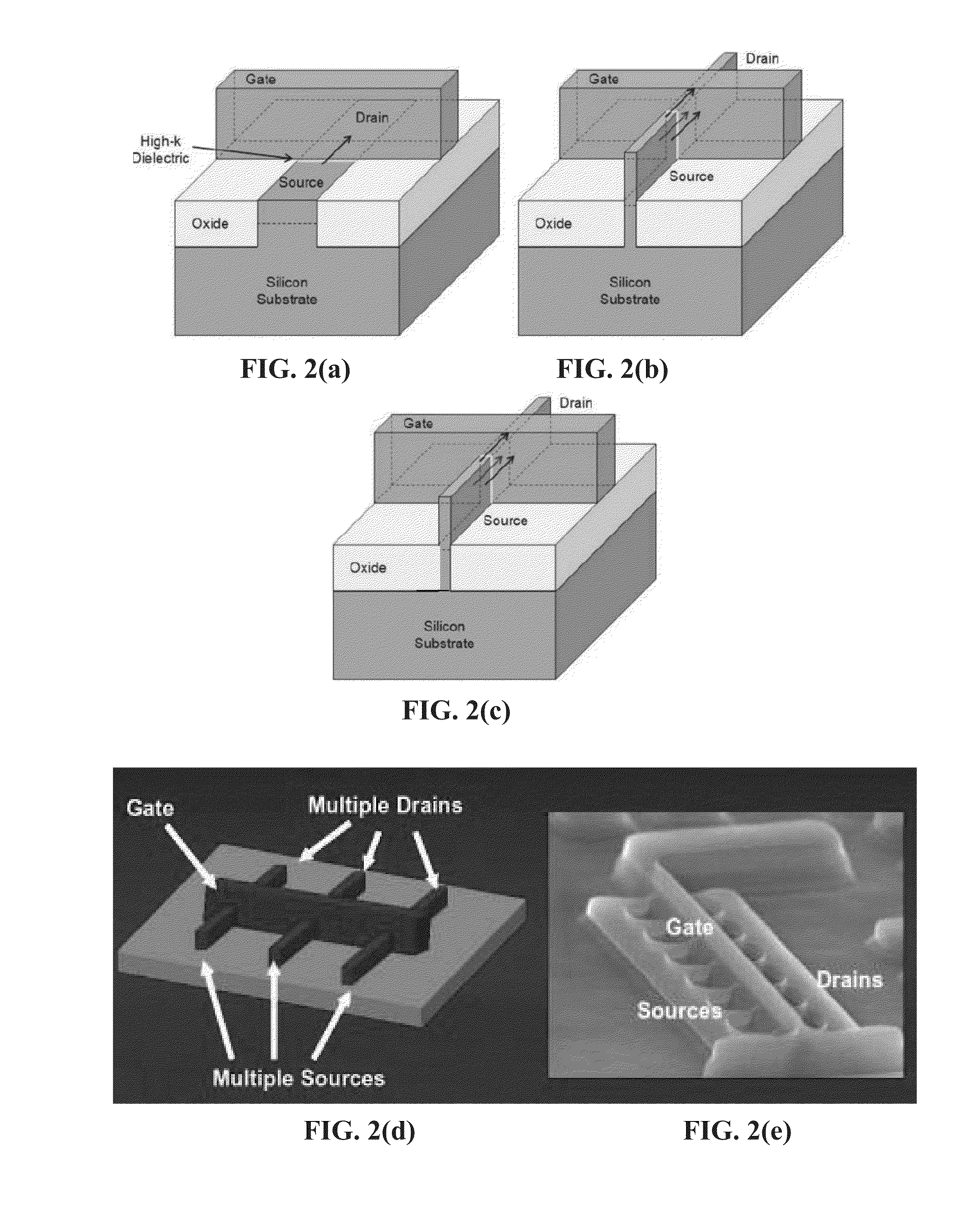
[0098]Embodiments disclosed herein use a junction diode or MOS in standard FinFET technologies as program selector for a programmable resistive device. The diode can comprise P+ and N+ active regions on an N well or on an isolated active region. Since the P+ and N+ active regions and N well and / or isolated active region are readily available in standard FinFET processes, these devices can be formed in an efficient and cost effective manner. For standard FinFET technologies, extended source / drain regions or part of fins are isolated active regions that can be used to construct diodes as program selectors or even One-Time Programmable (OTP) element. There are no additional masks or process steps to save costs. The programmable resistive device can also be included within an electronic system.

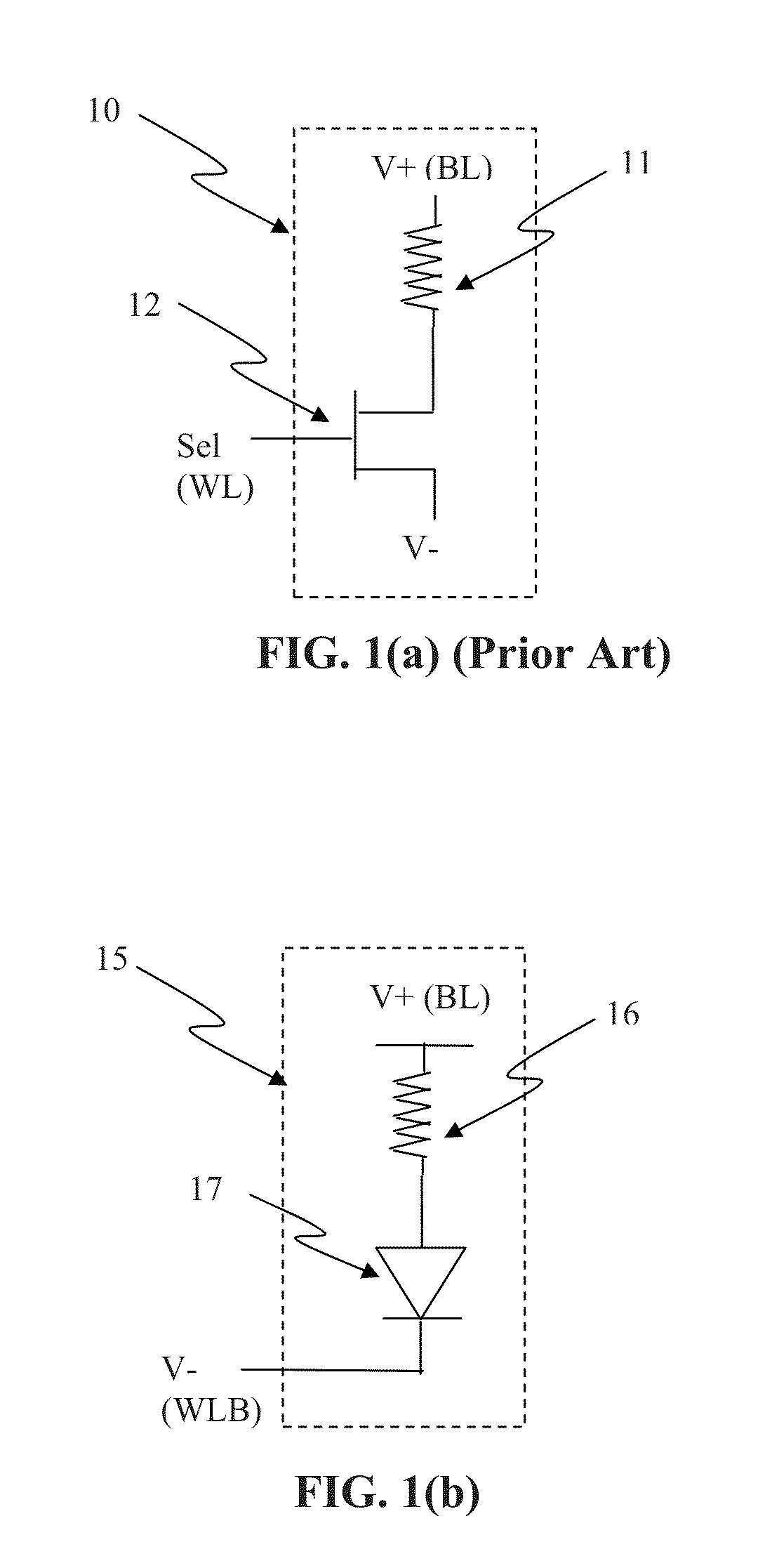
[0099]FIG. 4 shows a block diagram of a memory cell 30 using a FinFET diode or MOS in FinFET structures or isolated active region as program selector coupled to a programmable resistive element, a...


PUM

PropertyMeasurementUnit
widthaaaaaaaaaa
lengthaaaaaaaaaa
lengthaaaaaaaaaa

Abstract

Junction diodes or MOS devices fabricated in standard FinFET technologies can be used as program selectors or One-Time Programmable (OTP) element in a programmable resistive device, such as interconnect fuse, contact/via fuse, anti-fuse, or emerging nonvolatile memory such as MRAM, PCRAM, CBRAM, or RRAM. The MOS or diode can be built on at least one fin structure or at least one active region that has at least one first active region and a second active region. The first and the second active regions can be isolated by a dummy MOS gate or silicide block layer (SBL) to construct a diode.

Description

CROSS-REFERENCE TO RELATED APPLICATIONS[0001]This application is a continuation-in-part of U.S. patent application Ser. No. 13 / 026,678, filed on Feb. 14, 2011 and entitled “MEMORY DEVICES USING A PLURALITY OF DIODES AS PROGRAM SELECTORS WITH AT LEAST ONE BEING A POLYSILICON DIODE,” which is hereby incorporated herein by reference.[0002]This application also claims priority benefit of U.S. Provisional Patent Application No. 61 / 595,165, filed on Feb. 6, 2012 and entitled “Novel One-Time Programmable Device In Standard FinFET Technologies,” which is hereby incorporated herein by reference.BACKGROUND OF THE INVENTION[0003]A programmable resistive device is generally referred to a device's resistance states that may change after means of programming. Resistance states can also be determined by resistance values. For example, a resistive device can be a One-Time Programmable (OTP) device, such as electrical fuse, and the programming means can apply a high voltage to induce a high current ...

Claims


Application Information

Patent Timeline
Patent Type & Authority Applications(United States)
IPC IPC(8): H01L45/00G11C13/00
CPCH01L45/04H01L27/1211H01L45/085H01L45/144H01L45/146H01L45/147H01L27/224H01L27/228H01L27/2409H01L27/2436H01L27/2463H01L27/2472G11C11/1659H01L45/1253H01L27/0924G11C2213/74G11C2213/72G11C2013/0073G11C17/16G11C13/0069G11C13/004G11C13/003G11C13/0028G11C13/0011G11C13/0007G11C13/0004G11C13/0002G11C11/1675H01L45/06H10B61/10H10B63/82H10B63/20H10B63/30H10B61/22H10B63/80H10N70/245H10N70/231H10N70/20H10N70/8836H10N70/8828H10N70/8833H10B63/34H10N70/253H10N70/826H10N70/841G11C13/0026G11C17/18
Inventor CHUNG, SHINE C.
Owner ATTOPSEMI TECH CO LTD
Why Eureka
Try Eureka