Surface treatment and deposition for reduced outgassing

a technology of surface treatment and deposition, applied in the direction of chemical vapor deposition coating, coating, plasma technique, etc., can solve the problems of dielectric material, dielectric material, and structural features of the device having decreased spatial dimensions,

Inactive Publication Date: 2013-06-13
APPLIED MATERIALS INC
View PDF20 Cites 33 Cited by
  • Summary
  • Abstract
  • Description
  • Claims
  • Application Information

AI Technical Summary

Problems solved by technology

The decreasing feature sizes result in structural features on the device having decreased spatial dimensions.
The widths of gaps and trenches on the device narrow to a point where the aspect ratio of gap depth to its width becomes high enough to make it challenging to fill the gap with dielectric material.
The depositing dielectric material is prone to clog at the top before the gap completely fills, producing a void or seam in the middle of the gap.
However, once these highly flowable materials are deposited, they have to be hardened into a solid dielectric material.
Unfortunately, the departing carbon and hydroxyl species often leave behind pores in the hardened dielectic that reduce the quality of the final material.
In addition, the hardening dielectric also tends to shrink in volume, which can leave cracks and spaces at the interface of the dielectric and the surrounding substrate.
High temperature exposure to oxygen environments can ruin underlying layers for some circuit architectures.
This consideration results in the need to stay within a “thermal budget” during a manufacturing process flow.
Thermal budget considerations have largely limited SOD to process flows incorporating an underlying silicon nitride layer which can protect underlying features from oxidation (e.g. DRAM applications).

Method used


Image

  • Surface treatment and deposition for reduced outgassing
  • Surface treatment and deposition for reduced outgassing
  • Surface treatment and deposition for reduced outgassing

Examples


Embodiment Construction

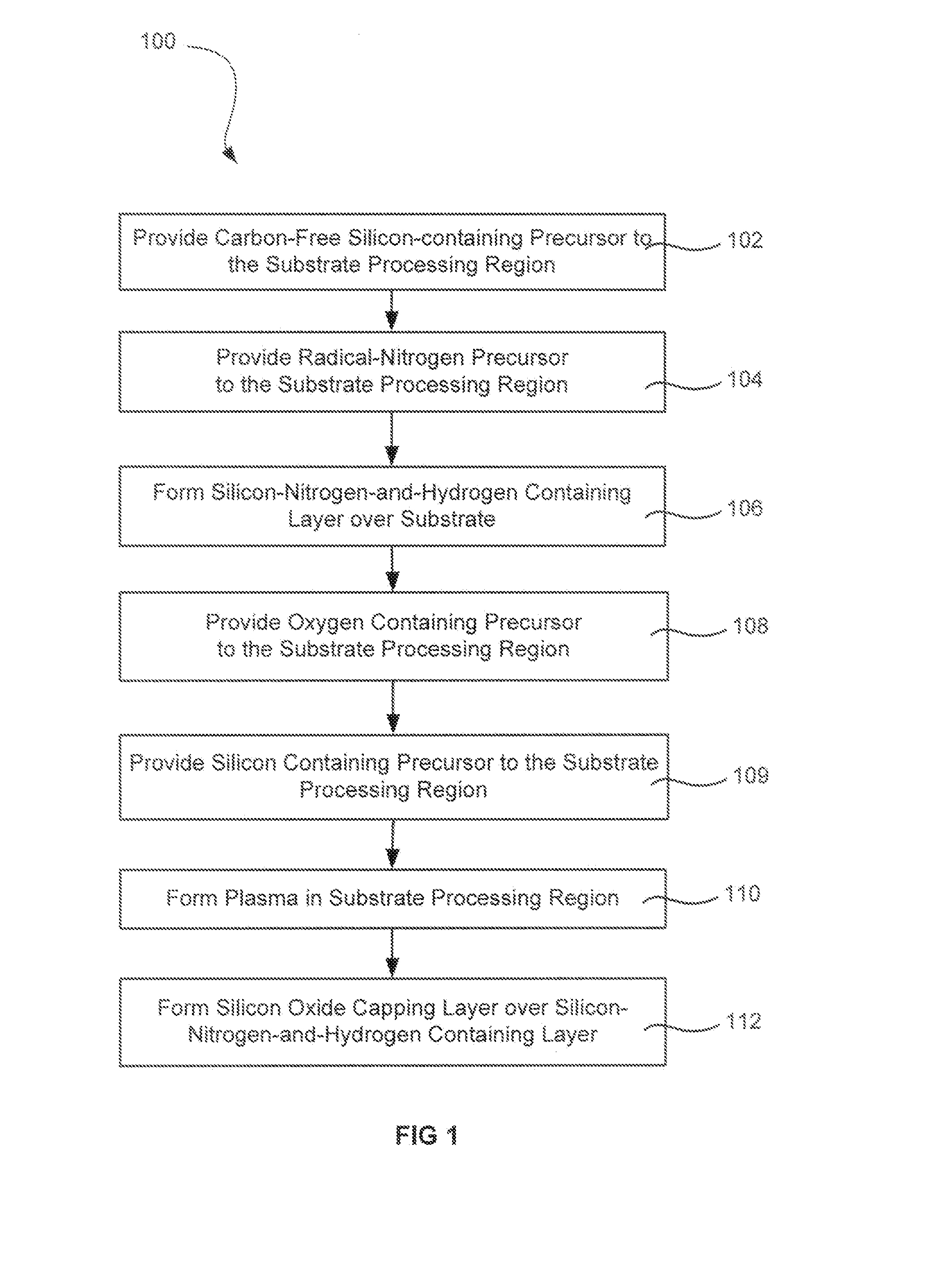
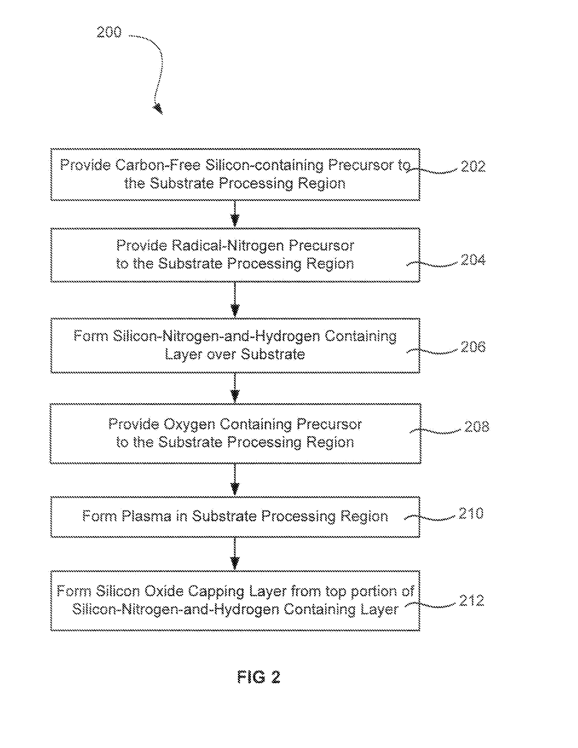
[0018]A method of forming a dielectric layer is described. The method first deposits a silicon-nitrogen-and-hydrogen-containing (polysilazane) layer by radical-component chemical vapor deposition (CVD). The silicon-nitrogen-and-hydrogen-containing layer is formed by combining a radical precursor (excited in a remote plasma) with an unexcited carbon-free silicon precursor. A silicon oxide capping layer may be formed from a portion of the carbon-free silicon-nitrogen-and-hydrogen-containing layer to avoid time-evolution of underlying layer properties prior to conversion into silicon oxide. Alternatively, the silicon oxide capping layer is formed over the silicon-nitrogen-and-hydrogen-containing layer. Either method of formation involves the formation of a local plasma within the substrate processing region.

[0019]Positioning a radical-component CVD silicon-nitrogen-and-hydrogen-containing layer beneath a silicon oxide capping layer has been found to reduce and / or eliminate outgassing a...


PUM

PropertyMeasurementUnit
temperatureaaaaaaaaaa

Abstract

A method of forming a dielectric layer is described. The method first deposits a silicon-nitrogen-and-hydrogen-containing (polysilazane) layer by radical-component chemical vapor deposition (CVD). The silicon-nitrogen-and-hydrogen-containing layer is formed by combining a radical precursor (excited in a remote plasma) with an unexcited carbon-free silicon precursor. A silicon oxide capping layer may be formed from a portion of the carbon-free silicon-nitrogen-and-hydrogen-containing layer to avoid time-evolution of underlying layer properties prior to conversion into silicon oxide. Alternatively, the silicon oxide capping layer is formed over the silicon-nitrogen-and-hydrogen-containing layer. Either method of formation involves the formation of a local plasma within the substrate processing region.

Description

CROSS-REFERENCES TO RELATED APPLICATIONS[0001]This application claims the benefit of U.S. Prov. Pat. App. No. 61 / 508,355 filed Jul. 15, 2011, and titled “SURFACE TREATMENT AND DEPOSITION FOR REDUCED OUTGASSING,” which is entirely incorporated herein by reference for all purposes.BACKGROUND OF THE INVENTION[0002]Semiconductor device geometries have dramatically decreased in size since their introduction several decades ago. Modern semiconductor fabrication equipment routinely produce devices with 45 nm, 32 nm, and 28 nm feature sizes, and new equipment is being developed and implemented to make devices with even smaller geometries. The decreasing feature sizes result in structural features on the device having decreased spatial dimensions. The widths of gaps and trenches on the device narrow to a point where the aspect ratio of gap depth to its width becomes high enough to make it challenging to fill the gap with dielectric material. The depositing dielectric material is prone to clo...

Claims


Application Information

Patent Timeline
Patent Type & Authority Applications(United States)
IPC IPC(8): C23C16/40
CPCC23C16/401H01L21/02164H01L21/0217H01L21/022C23C16/56C23C16/345C23C16/452C23C16/45565C23C16/505H01L21/02274C23C16/45514
Inventor LIANG, JINGMEICHEN, XIAOLININGLE, NITIN K.VENKATARAMAN, SHANKAR
Owner APPLIED MATERIALS INC
Why Eureka
Try Eureka