
Process for Hybrid Integration of Focal Plane Arrays

a focal plane array and hybridization technology, applied in the field of focal plane array hybridization, can solve the problems of reducing the surface energy of solder bumps, limiting the alignment accuracy that can be achieved with a conventional die bonder, and many commonly used solders having a melting point that is higher

Inactive Publication Date: 2013-06-20
PRINCETON LIGHTWAVE INC
View PDF18 Cites 13 Cited by
  • Summary
  • Abstract
  • Description
  • Claims
  • Application Information

AI Technical Summary

Benefits of technology

The present invention is a method for joining two substrates with each other using solder bumps that include indium. The method involves reducing surface oxide on the solder bumps, arranging the substrates so that they are physically coupled via the solder bumps, and then reflowing the solder bumps to enable a reduction of surface energy. The technical effects of this invention include improved bonding efficiency and reduced surface energy of the solder bumps, resulting in a more robust and reliable bond.

Problems solved by technology

Unfortunately, conventional flip-chip solder-bump bonding has several drawbacks for many applications—especially the integration of optical devices, such as a focal-plane array (FPA) onto its control circuit, such as a Read-Out Integrated Circuit (ROIC).
First, the alignment accuracy that can be attained with a conventional die bonder is limited to a few microns, which is insufficient for integrating a highly dense, small pixel-element FPA onto an ROIC.
Second, many commonly used solders have a melting point that is higher than the thermal budget of either the FPA or the ROIC.
This is particularly problematic for single-photon detection devices, which include very shallow diffusion regions.

Method used


Image

  • Process for Hybrid Integration of Focal Plane Arrays
  • Process for Hybrid Integration of Focal Plane Arrays
  • Process for Hybrid Integration of Focal Plane Arrays

Examples


Embodiment Construction

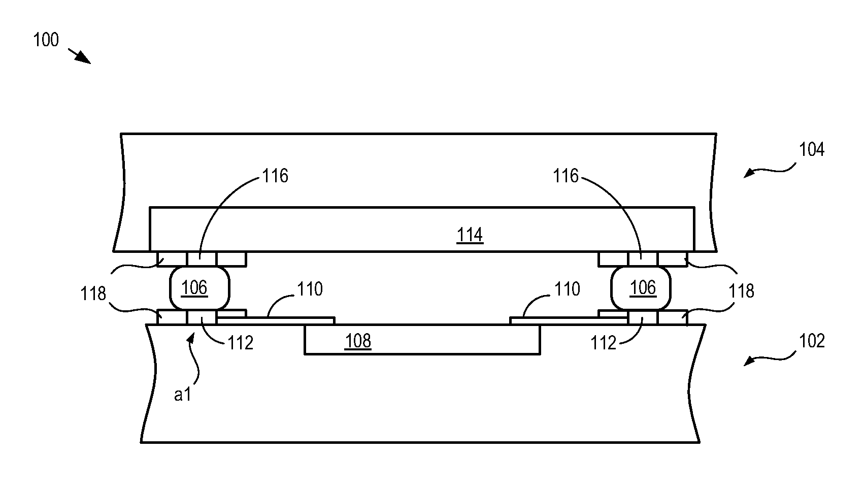
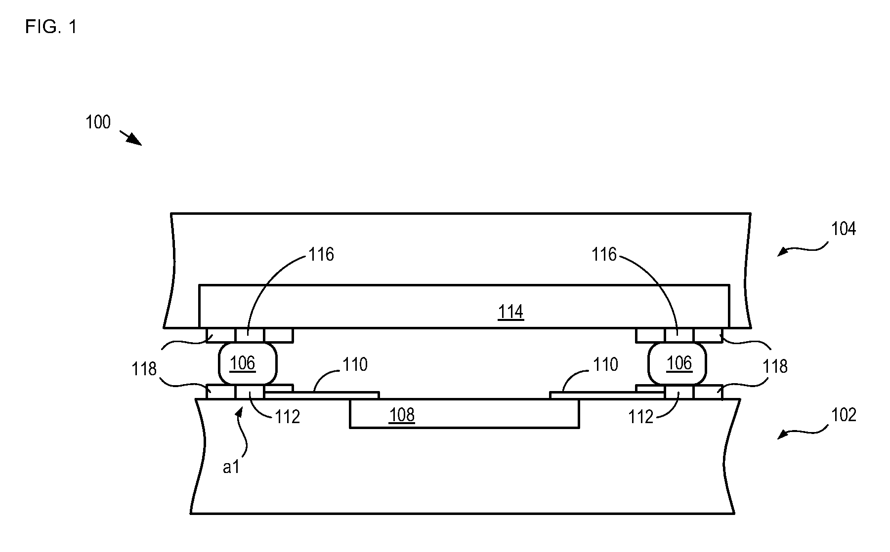
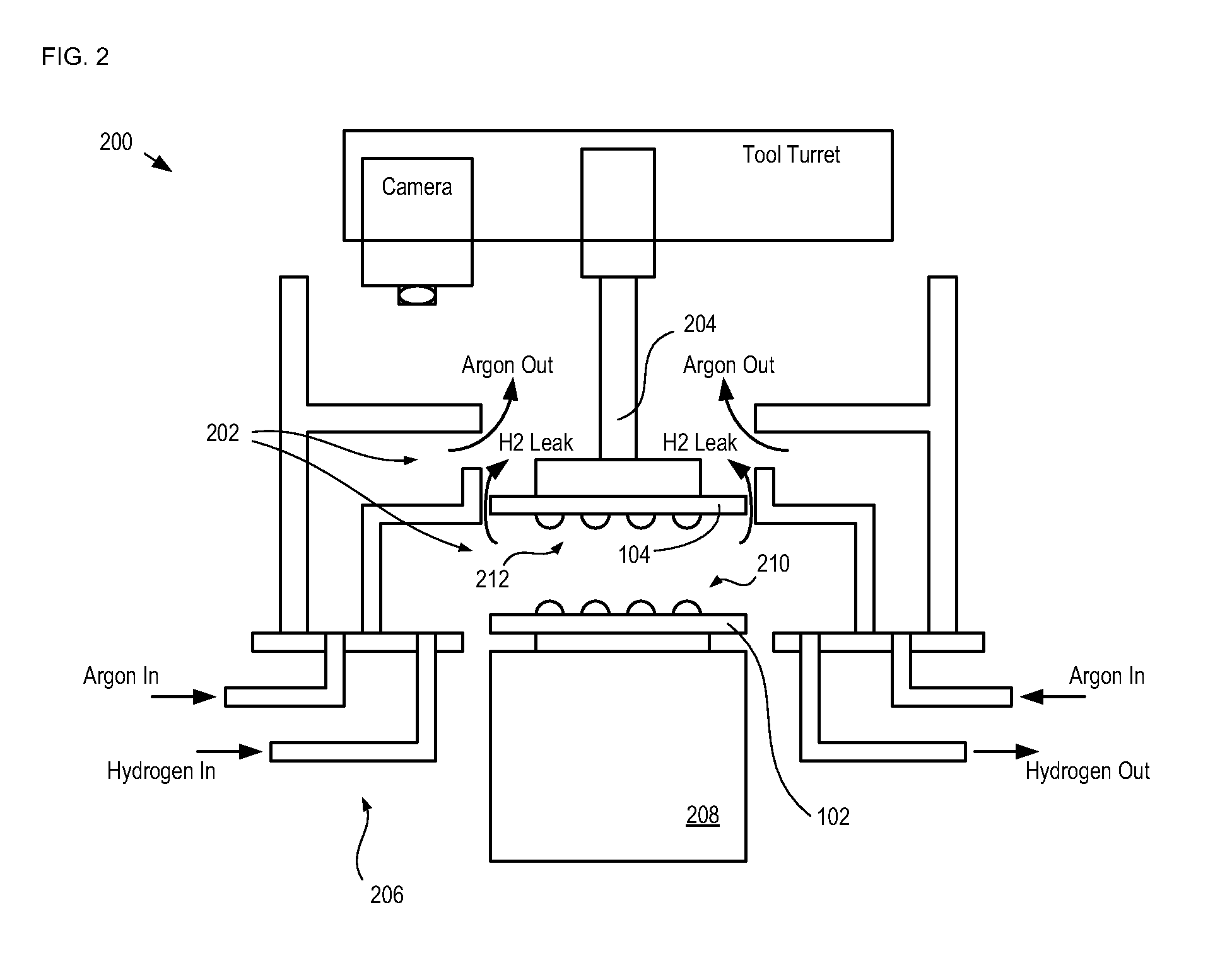
[0016]It is an aspect of the present invention that solder-reflow after flip-chip solder-bump bonding can be used to improve the alignment accuracy between two substrates. Since most solders have a melting point that is higher than the thermal budget of a typical PFA, however, it is a further aspect of the present invention to use indium-based solder bumps (including pure indium), which have a low melting point. It is well known, however, that indium-base solders quickly develop a surface oxide that inhibits their use in bump bonding applications. It is a further aspect of the present invention, therefore, that reduction of the surface oxide on indium-based solder bumps is done while the solder bumps are contained within a chamber having a controllable environment. A pick-and-place tool having access into the chamber is then used to roughly align and bond the two substrates once the surface oxide is sufficiently reduced. After bonding, the two substrates are heated to melt the indiu...


PUM


Abstract

A method for aligning a first substrate relative to a second substrate by enabling reflow of low-melting-temperature solder bumps is disclosed. Reflow of the solder bumps induces a force that moves one substrate relative to the other to improve alignment accuracy between bond pads located on each substrate. The method further enables reduction of surface oxide on the solder bumps that would otherwise inhibit reliable solder joint formation.

Description

CROSS REFERENCE TO RELATED APPLICATIONS[0001]This case claims priority of U.S. Provisional Patent Application U.S. 61 / 561,151, which was filed on Nov. 17, 2011 (Attorney Docket: 293-028PROV), and which is incorporated herein by reference.STATEMENT REGARDING FEDERALLY SPONSORED RESEARCH[0002]This invention was made with Government support under contract FA8650-10-1727 awarded by the United States Air Force. The Government has certain rights in the invention.FIELD OF THE INVENTION[0003]The present invention relates to focal plane arrays in general, and, more particularly, to hybrid integration of focal plane arrays and read-out integrated circuits.BACKGROUND OF THE INVENTION[0004]Hybrid integration of two substrates using flip-chip solder-bump bonding has been a mainstay of the semiconductor industry for decades. In such integration, a first substrate comprising a first type of semiconductor device flipped over and attached to a second substrate by means of solder bumps that interpose...

Claims


Application Information

Patent Timeline
Patent Type & Authority Applications(United States)
IPC IPC(8): H01L23/00
CPCH01L24/81H01L2224/83193H01L2224/81815H01L2224/81121H01L2224/81065H01L2224/75753H01L2224/75251H01L2224/13109H01L25/50H01L2225/06513H01L27/14634H01L27/14636H01L2224/75101H01L2224/75272H01L24/13H01L24/75H01L2224/13101H01L2924/01001H01L2924/014H01L2924/00014H01L2924/01322H01L2924/00
Inventor OWENS, MARK ANDREWRANGWALA, SABBIR SAJJADONAT, BORA MUAMMERSALVEMINI, DOMENICK
Owner PRINCETON LIGHTWAVE INC
Learn More