Flux-free chip to wafer joint serial thermal processor arrangement

US20110198388A1Inactive Publication Date: 2011-08-18SEMLGEAR INC

Image

  • Flux-free chip to wafer joint serial thermal processor arrangement
  • Flux-free chip to wafer joint serial thermal processor arrangement
  • Flux-free chip to wafer joint serial thermal processor arrangement

Examples


Embodiment Construction

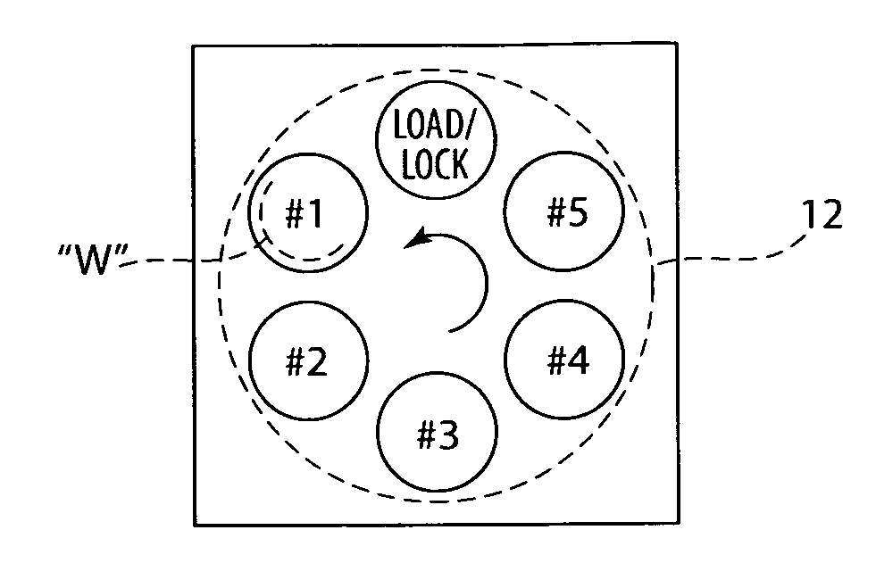
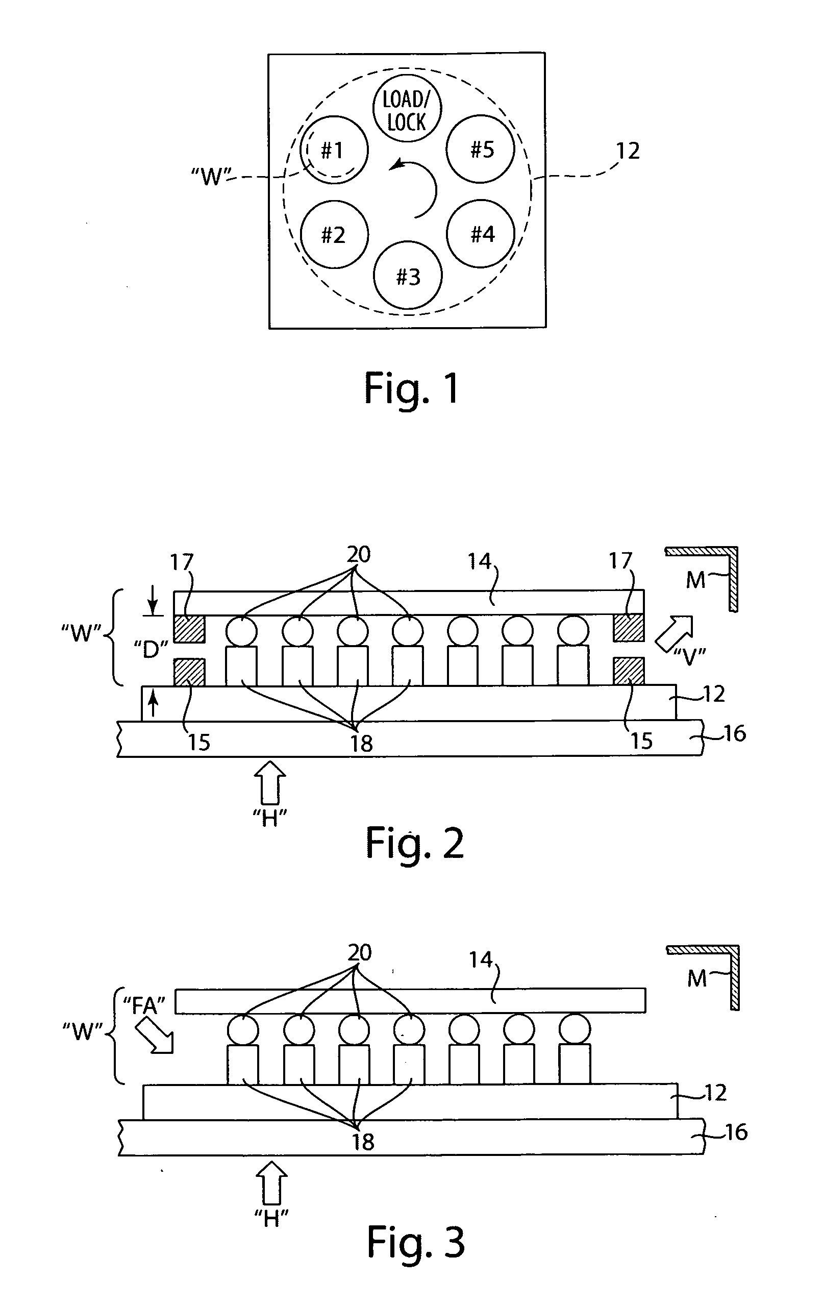
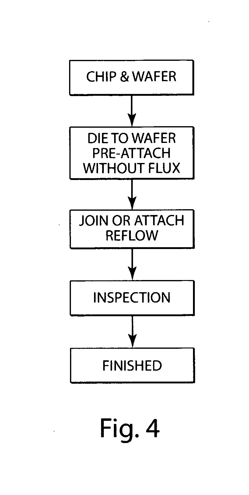
[0049]The invention a an electronic chip and chip manufacturing process which comprises a rotatable, circumferentially organized, serial thermal processing station arrangement 10 using a method for serially treating a pre-assembled chip or die and a wafer assembly “W” through a series of preferably at least six independent, enclosed station chambers in the processor arrangement 10, as represented in FIG. 1.

[0050]The rotary production station arrangement 10 is arranged to rotate so as to present a material to be treated, such as a semiconductor wafer, at a series of circumferentially spaced-apart locations, from a Load / Lock station to processing stations numbered 1 through 5, which stations each are arranged to independently control the temperature, pressure and atmosphere thereat, as is similarly represented in various aspects and embodiments of the arrangement 10, in a mechanism as may be shown in the above-identified '789 and '879 patents, incorporated by reference herein.

[0051]Th...


PUM

PropertyMeasurementUnit
Temperatureaaaaaaaaaa

Abstract

A serial thermal processing arrangement for treating a pre-assembled chip / wafer assembly of semiconductor material in a rotary processor, through a series of intermittent, rotatively advanced, movements into independent, temperature and pressure controlled, circumferentially disposed chambers,

Description

BACKGROUND OF THE INVENTION[0001]1. Field of the Invention[0002]The present invention relates to an electronic chip and to a method of manufacturing same such as semiconductor wafers and more particularly to a stepwise process of a machine utilized in that manufacture of semiconductor wafers and is a continuation-in-part application of co-pending U.S. patent application Ser. No. xx / yyy,yyy (Semigear-22) filed concurrently herewith, and wherein the present application claims the benefit of and is a CIP of Ser. No. 12 / 653,454, filed Dec. 14, 2009, which is a division of Ser. No. 11 / 482,838, filed Jul. 7, 2006, now U.S. Pat. No. 7,632,750, which is a CIP of Ser. No. 10 / 832,782, filed Apr. 27, 2004, now U.S. Pat. No. 7,008,879, which is a division of Ser. No. 10 / 186,823, filed Jul. 1, 2002, now U.S. Pat. No. 6,827,789, each incorporated herein by reference in the present Application.[0003]2. Description of the Prior Art[0004]Formation of a solder bump on a semiconductor substrate takes ...

Claims


Application Information

Patent Timeline
18 Aug 2011
Publication
US20110198388A1
IPC
B23K3/08; B23K3/04; B23K37/04
CPC
B23K3/0623; B23K2201/40; H01L24/11; H01L24/742; H01L2224/16; H01L2924/01027; H01L2924/01029; H01L2924/01047
Inventors
ZHANG, JIAN