Methods for fabricating nanocrystalline diamond film

a nanocrystalline diamond and thin film technology, applied in the direction of polycrystalline material growth, mechanical vibration separation, water-setting substance layered product, etc., can solve the problems of limited diamond deposition, difficult to grow a void-free nanocrystalline diamond thin film on the silicon oxide surface, and inconvenient technique for non-conducting substrates such as oxide-coated substrates, etc., to maximize electrostatic attraction and minimize voids

Inactive Publication Date: 2015-07-07
KOREA INST OF SCI & TECH
View PDF8 Cites 0 Cited by
  • Summary
  • Abstract
  • Description
  • Claims
  • Application Information

AI Technical Summary

Benefits of technology

[0012]Embodiments are directed to providing a uniform nanocrystalline diamond thin film with minimized voids formed on a silicon oxide-coated substrate by performing hydrogen plasma treatment, hydrocarbon plasma treatment or hydrocarbon thermal treatment on the substrate surface to maximize electrostatic attraction between the substrate surface and nanodiamond particles during the following ultrasonic seeding such that the nanodiamond particles are uniformly distributed and bound on the silicon oxide on the substrate and a method for fabricating same.

Problems solved by technology

Meanwhile, it is very difficult to grow a void-free nanocrystalline diamond thin film on the silicon oxide surface due to low nucleation density and long pretreatment time when compared to the growth on the pristine silicon substrate (Bhattacharyya, S.; Auciello, O.; Birrell, J.; Carlisle, J. A.; Curtiss, L. A.; Goyette, A. N.; Gruen, D. M,; Krauss, A. R.; Schlueter, J.; Sumant, A.; Zapol, P.
However, although it is appropriate for an electrically conducting substrate, the technique is not suitable for a non-conducting substrate such as an oxide-coated substrate and is limited in large-area diamond deposition.
However, such efforts are directed exclusively to the diamond particles, not to the substrate onto which the diamond particles are transferred.

Method used


Image

  • Methods for fabricating nanocrystalline diamond film
  • Methods for fabricating nanocrystalline diamond film
  • Methods for fabricating nanocrystalline diamond film

Examples


example 1

Experimental Methods

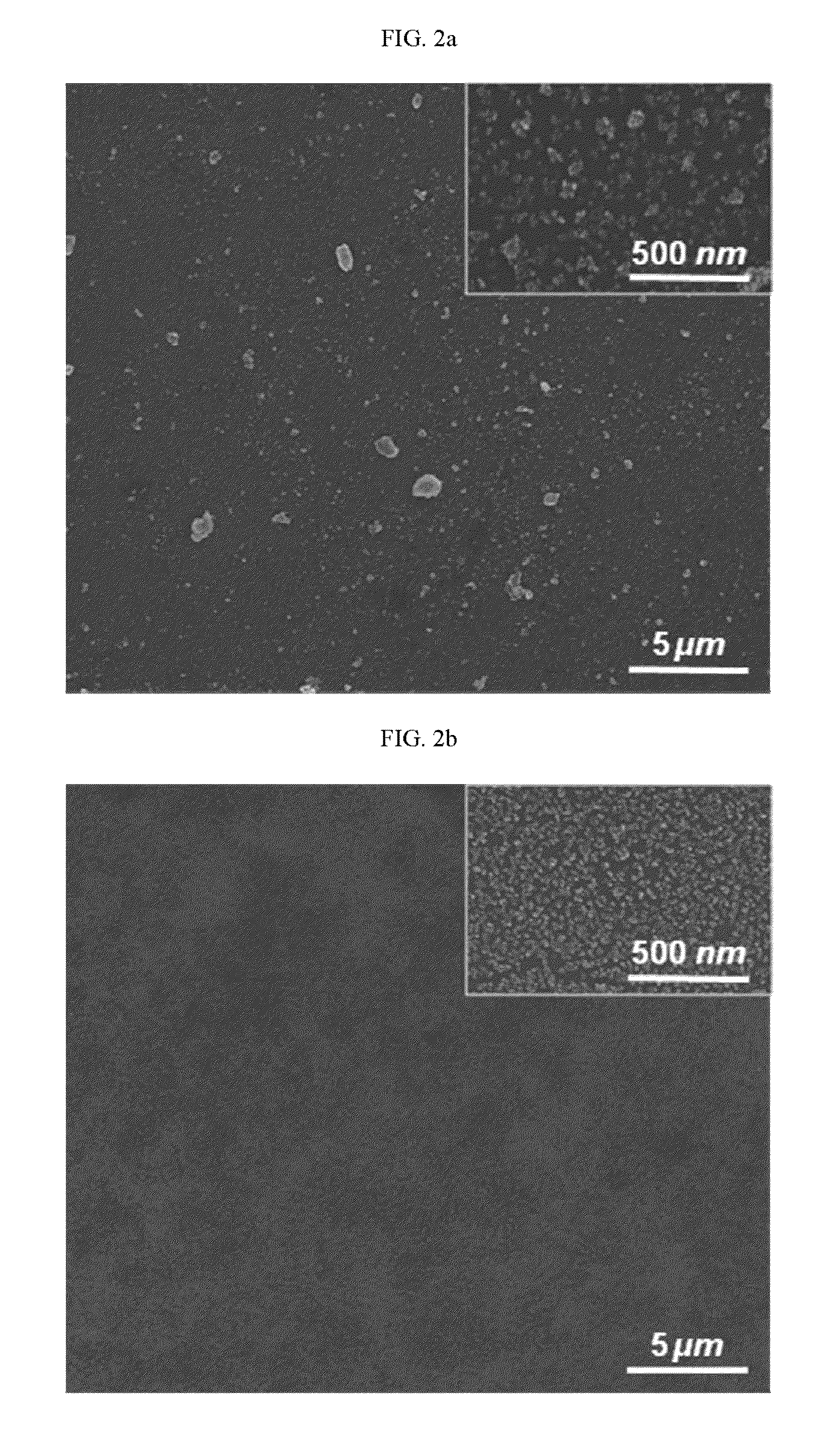
[0052]A silicon oxide (SiO2)-coated silicon substrate was treated with a hydrogen plasma (*), treated with a hydrogen plasma and a hydrocarbon plasma (**) or thermally treated in the presence of a mixture gas of hydrogen and hydrocarbon (***). Subsequently, the substrate was ultrasonically seeded (ultrasonic treatment) and the binding of the nanodiamond particles was characterized. After the ultrasonic seeding, a nanocrystalline diamond film was grown by chemical vapor deposition (UNCD deposition) and characterized. Also, a nanocrystalline diamond film was grown on a silicon substrate (bare Si) and a silicon oxide (SiO2)-coated silicon substrate (bare SiO2 / Si), which were not surface-treated.

[0053]During the ultrasonic seeding, the zeta potential of the nanodiamond particles and the zeta potential of the substrate were measured, with the surface-treated substrate immersed in the suspension of nanodiamond particles, and the result was compared with the zeta potent...

example 2

Experimental Result

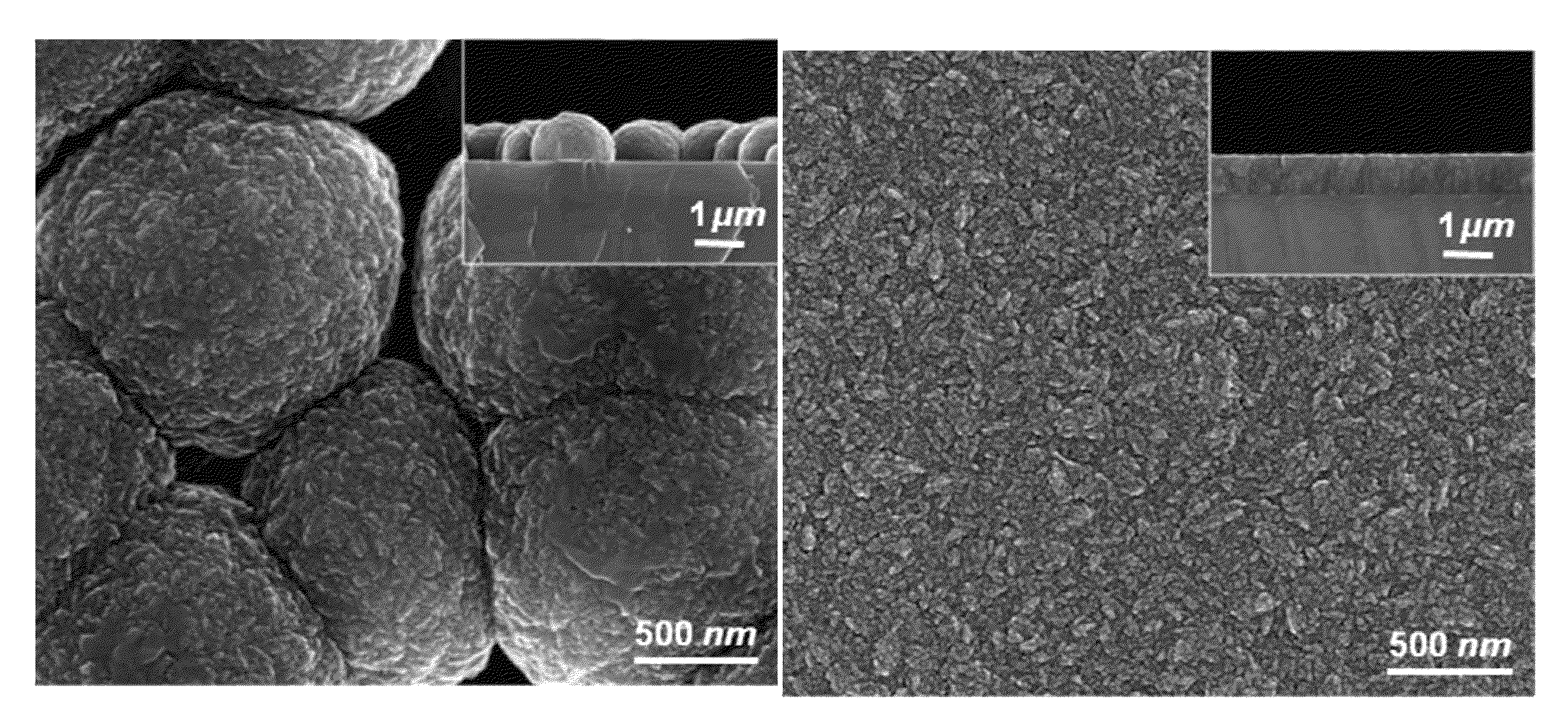
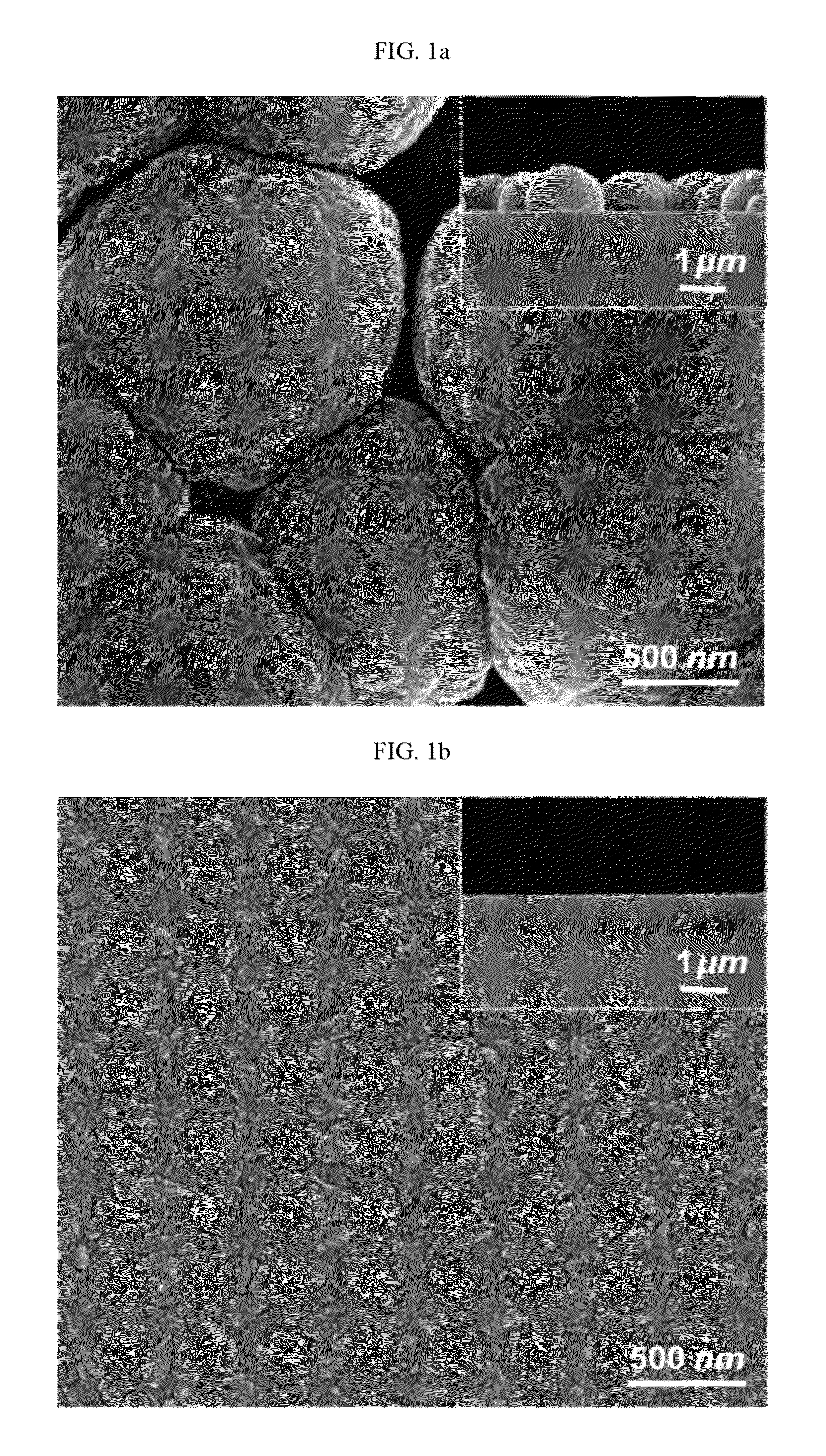
[0056]FIGS. 1a and 1b show scanning electron microscope (SEM) images of nanocrystalline diamond grown on a silicon oxide-coated silicon substrate (bare SiO2 / Si) and a silicon substrate (bare Si), which were not surface-treated. The nanocrystalline diamond was synthesized for 4 hours by DC-PACVD and other experimental condition was the same as that of the nanocrystalline diamond growth in Example 1.

[0057]Referring to FIG. 1a, a discontinuous diamond thin film comprising clusters with a diameter of 1 μm or larger was grown on the bare SiO2 / Si. Referring to FIG. 1b, a well-defined continuous diamond thin film was grown on the bare Si. This indicates that the initial nucleation density is much lower for the bare SiO2 / Si substrate as compared to the bare Si substrate. The same result was observed when the film was grown by thermal deposition (HFCVD) not by the plasma deposition (DC-PACVD). Accordingly, improvement of the nucleation density is necessary to synthesize a ...


PUM

PropertyMeasurementUnit
thicknessaaaaaaaaaa
thicknessaaaaaaaaaa
diameteraaaaaaaaaa

Abstract

Methods for fabricating uniform nanocrystalline diamond thin films with minimized voids are presented. These uniform nanocrystalline diamond thin films can be formed on any number of treated silicon oxide surfaces such as on hydrogen plasma treated surfaces of silicon oxide-coated substrates or on hydrocarbon plasma pre-treated surfaces of silicon oxide-coated substrates. It is believed that treating these surfaces results in maximizing electrostatic attraction between these treated surfaces with nanodiamond particles during a subsequent ultrasonic seeding of the nanodiamond particles onto these threated surfaces. This can result in the nanodiamond particles being substantially uniformly distributed and bound on the treated silicon oxide surface.

Description

CROSS-REFERENCE TO RELATED APPLICATION[0001]This application claims priority to Korean Patent Application No. 10-2012-0031830, filed on Mar. 28, 2012, and all the benefits accruing therefrom under 35 U.S.C. §119, the contents of which in its entirety are herein incorporated by reference.BACKGROUND[0002]1. Field[0003]Embodiments relate to a nanocrystalline diamond thin film and a method for fabricating same. More particularly, embodiments relate to a uniform nanocrystalline diamond thin film with minimized voids formed on a silicon oxide-coated substrate and a method for fabricating the same. Such nanocrystalline diamond thin film is formed by performing hydrogen plasma treatment, hydrocarbon plasma treatment or hydrocarbon thermal treatment on the substrate surface to maximize electrostatic attraction between the substrate surface and nanodiamond particles during the following ultrasonic seeding such that the nanodiamond particles are uniformly distributed and bound on the silicon o...

Claims


Application Information

Patent Timeline
Patent Type & Authority Patents(United States)
IPC IPC(8): C23C16/27C23C16/02
CPCC23C16/27C23C16/02C23C16/0254C23C16/271C23C16/272C23C16/0218C23C16/0245C23C16/0272C30B29/04
Inventor LEE, WOOK SEONGLEE, HAK JOOBAIK, YOUNG JOONPARK, JONG KEUK
Owner KOREA INST OF SCI & TECH
Why Eureka
Try Eureka