LED lens and light emitting device using the same

a technology of light-emitting devices and lenses, which is applied in the direction of semiconductor devices, lighting and heating apparatus, instruments, etc., can solve the problems of difficult to achieve high light-scattering ability and uniform light distribution of light source devices simultaneously, and light patterns with higher intensities in the paraxial region, so as to improve illumination uniformity and effective divergence angle

Active Publication Date: 2013-06-20
E PIN OPTICAL IND
View PDF1 Cites 47 Cited by
  • Summary
  • Abstract
  • Description
  • Claims
  • Application Information

AI Technical Summary

Benefits of technology

[0012]An aspect of the present disclosure is to provide an LED lens and a light emitting device applied to an LED backlight module or other illumination device...

Problems solved by technology

Therefore, in the LCD display using LEDs as backlight source, the way to enhance the uniformity of brightness or make the light distribution be wider is the main issue for improving the LED backlight device.
These kinds of issues are unlikely to be overcome due to an uneven distribution of emission intensity of the light source device 1.
In a result, the light source device 1 is hard to have a high light-scattering ability and a uniformity of light distribution simultaneously.
However, optical structures disclosed in the two patent documents also cause a light pattern with higher intensities in the paraxial region thereof.
Therefore, the requirements of light distribution uniformity and light scattering ability are hard to meet.
However, such optical lens is still hard to use in a thin display due to the limit of its optical structure.
In a result, such optical lens is not applicable to use in thin displays.
However, such light source devices are unlikely to ...

Method used


Image

  • LED lens and light emitting device using the same
  • LED lens and light emitting device using the same
  • LED lens and light emitting device using the same

Examples


first example

[0071]FIG. 8 is a cross-sectional view illustrating a light emitting device of the first example according to the present disclosure. In the first example, the light emitting surface 41 of the LED lens 4 has a shape according to table (1) listed below that shows coefficients of the aspheric surface formula (7).

TABLE (1)curvature (c)KA2A4A6A8A10A12−6.42E+12−2.23E+062.01E−02−1.44E−032.08E−05−4.89E−079.44E−09−9.54E−11

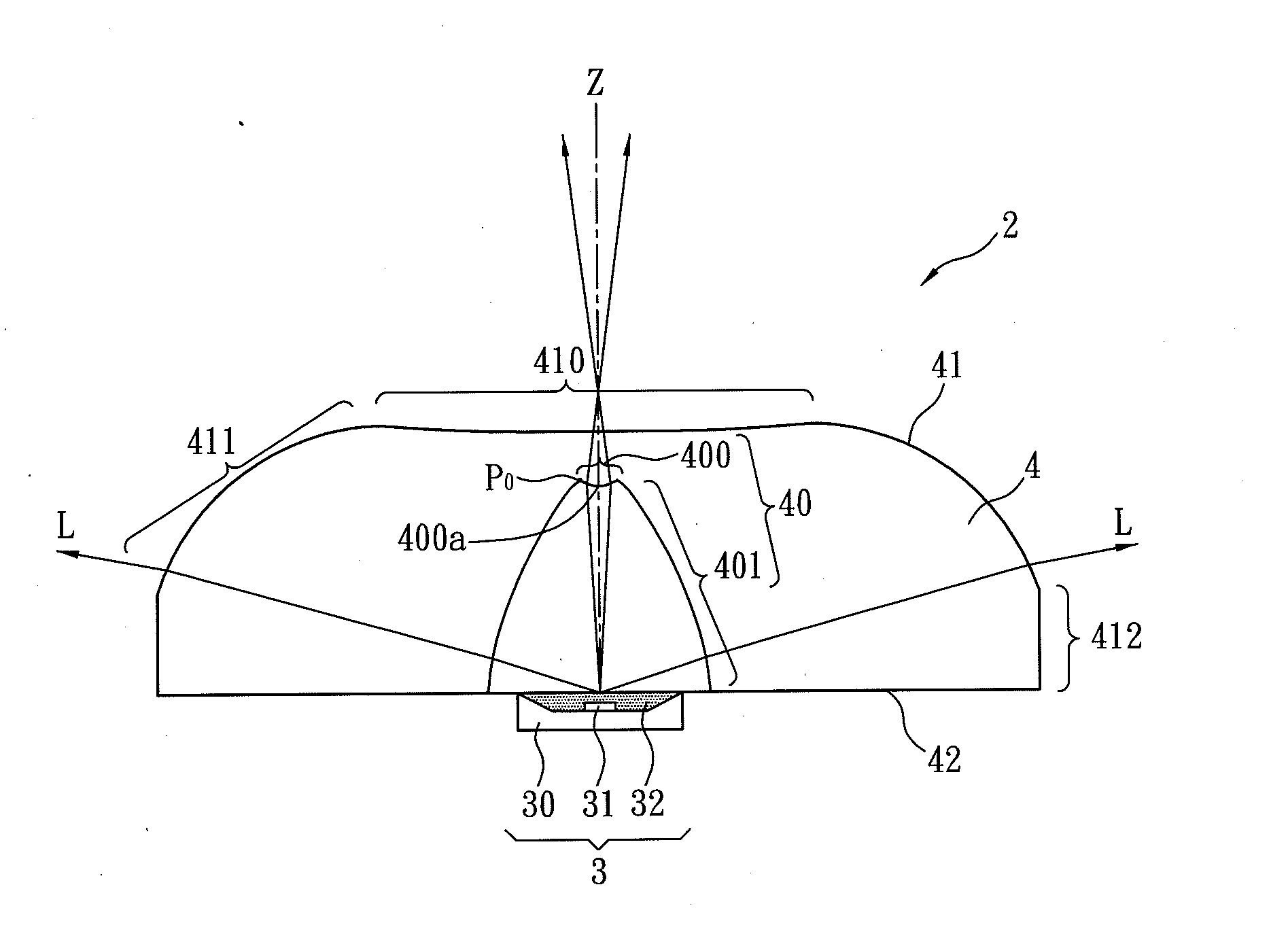
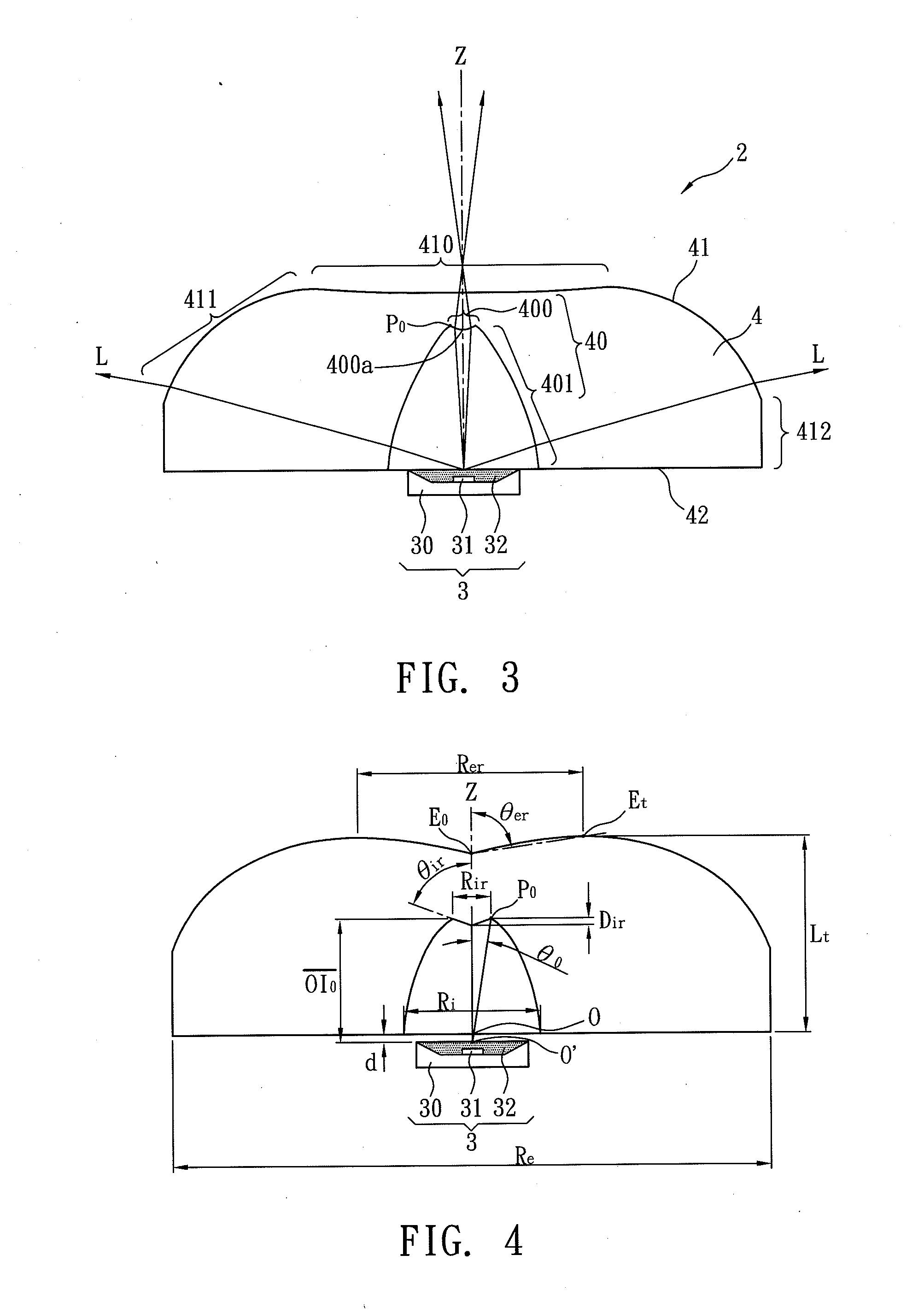
[0072]In Table (2) listed below, it shows the refractive index (Nd) of the LED lens 4, the data referred to FIG. 4, and the space distance (d) between the first plane and the second plane is located in the first example.

TABLE (2)Lt (mm)Re (mm)Rer (mm)tanθerRi (mm)Rir (mm)OI0 (mm)θT (°)4.69415.2005.66012.9263.5000.4682.25071tanθ0Sir (mm)OP0 (mm)Dir (mm)tanθird (mm)NdθM (°)0.0970.3112.4250.1641.430−0.8001.49156

[0073]In the first example, the first optically active area 400 of the light incident surface 40 is a concave surface. For detail description of the concave surface of...

second example

[0076]FIG. 9 is a cross-sectional view illustrating a light emitting device of the second example according to the present disclosure. In the second example, the light emitting surface 41 of the LED lens 4 has a shape according to table (3) listed below that shows coefficients of the aspheric surface formula (7).

TABLE (3)curvature (c)KA2A4A6A8A10A12−6.42E+12−2.23E+062.01E−02−1.44E−032.08E−05−4.89E−079.44E−09−9.54E−11

[0077]In Table (4) listed below, it shows the refractive index (Nd) of the LED lens 4, the data referred to FIG. 4, and the space distance (d) in the second example.

TABLE (4)Lt (mm)Re (mm)Rer (mm)tanθerRi (mm)Rir (mm)OI0 (mm)θT (°)4.72615.5005.36035.3843.6000.6202.74570tanθ0Sir (mm)OP0 (mm)Dir (mm)tanθird (mm)NdθM (°)0.1050.3702.9610.2001.5530.0001.49156

[0078]In the second example, the first optically active area 400 of the light incident surface 40 is a concave surface. For detail description of the concave surface of the light incident surface 40, it drops from the opt...

third example

[0081]FIG. 10 is a cross-sectional view illustrating a light emitting device of the third example according to the present disclosure. In the third example, the light emitting surface 41 of the LED lens 4 has a shape according to table (5) listed below that shows coefficients of the aspheric surface formula (7).

TABLE (5)curvature (c)KA2A4A6A8A10A12−6.42E+12−2.23E+062.01E−02−1.44E−032.08E−05−4.89E−079.44E−09−9.54E−11

[0082]In Table (6) listed below, it shows the refractive index (Nd) of the LED lens 4, the data referred to FIG. 4, and the space distance (d) in the third example.

TABLE (6)Lt (mm)Re (mm)Rer (mm)tanθerRi (mm)Rir (mm)OI0 (mm)θT (°)4.69415.5005.36049.6043.8000.6163.19471tanθ0Sir (mm)OP0 (mm)Dir (mm)tanθird (mm)Ndθm (°)0.0920.3443.3620.1541.9990.2001.49156

[0083]In the third example, the first optically active area 400 of the light incident surface 40 is a concave surface. For detail description of the concave surface of the light incident surface 40, it drops from the optica...


PUM


Abstract

An LED lens and a light emitting device using the same are disclosed. The LED lens comprises a light incident surface, a light emitting surface, and a bottom surface. The light emitting surface includes a first recession portion disposed at the central thereof and a protrusion portion connected to the outer periphery of the emitting recession portion. The light incident surface comprises a first optically active area and a second optically active area. The first optically active area is disposed at the central of the light incident surface, and has a second recession portion; the second optically active area is a concave surface connected to the first optically active area. The LED lens satisfies specific conditions. The LED lens distributes a light beam emitted from the light emitting device to form an even light pattern.

Description

FIELD OF THE INVENTION[0001]The present invention relates to a lens and a light emitting device using the same, and more particularly to an LED lens and a light emitting device applied for various illumination devices using light-emitting diodes (LEDs) as light source.BACKGROUND OF THE INVENTION[0002]LCD displays are widely used in TVs, laptop computers, PCs, mobile phones, and other electronic products having display function. In an LCD display, cold cathode fluorescent lamp (CCFL), field-effect light-emitting device (EL), light-emitting diode (LED), or other elements capable of emitting a visible light are used as a backlight. In recent years, LED has gradually become a preferred backlight source instead of CCFL because of its various advantages including: long lifetime (about 100,000 hours), capability of optimizing color gamut, small size / design flexibility, low-voltage power supply driven, short turn-on time, no inverter needed, efficiently operated over a wider temperature ran...

Claims


Application Information

Patent Timeline
IPC IPC(8): F21V5/04
CPCG02F2001/133607G02B19/0014G02B19/0061G02F1/133603F21Y2101/02F21V5/04F21Y2115/10G02F1/133607
Inventor CHEN, HUANG-CHANGWANG, CHIH-PENGHSU, KUO-HSUAN
Owner E PIN OPTICAL IND
Why Eureka
Try Eureka