Fiber to Wafer Interface

a fiber and wafer technology, applied in the direction of optics, optical waveguide light guides, instruments, etc., can solve the problems of inefficiency and cost of manufacture of the previous method and device for connecting optical devices to devices on wafers

Inactive Publication Date: 2013-06-20
IBM CORP +1
View PDF10 Cites 21 Cited by
  • Summary
  • Abstract
  • Description
  • Claims
  • Application Information

AI Technical Summary

Problems solved by technology

Previous methods and devices for connecting optical devices to devices on wafers are often inefficient and costly to manufacture.

Method used


Image

  • Fiber to Wafer Interface
  • Fiber to Wafer Interface
  • Fiber to Wafer Interface

Examples


Embodiment Construction

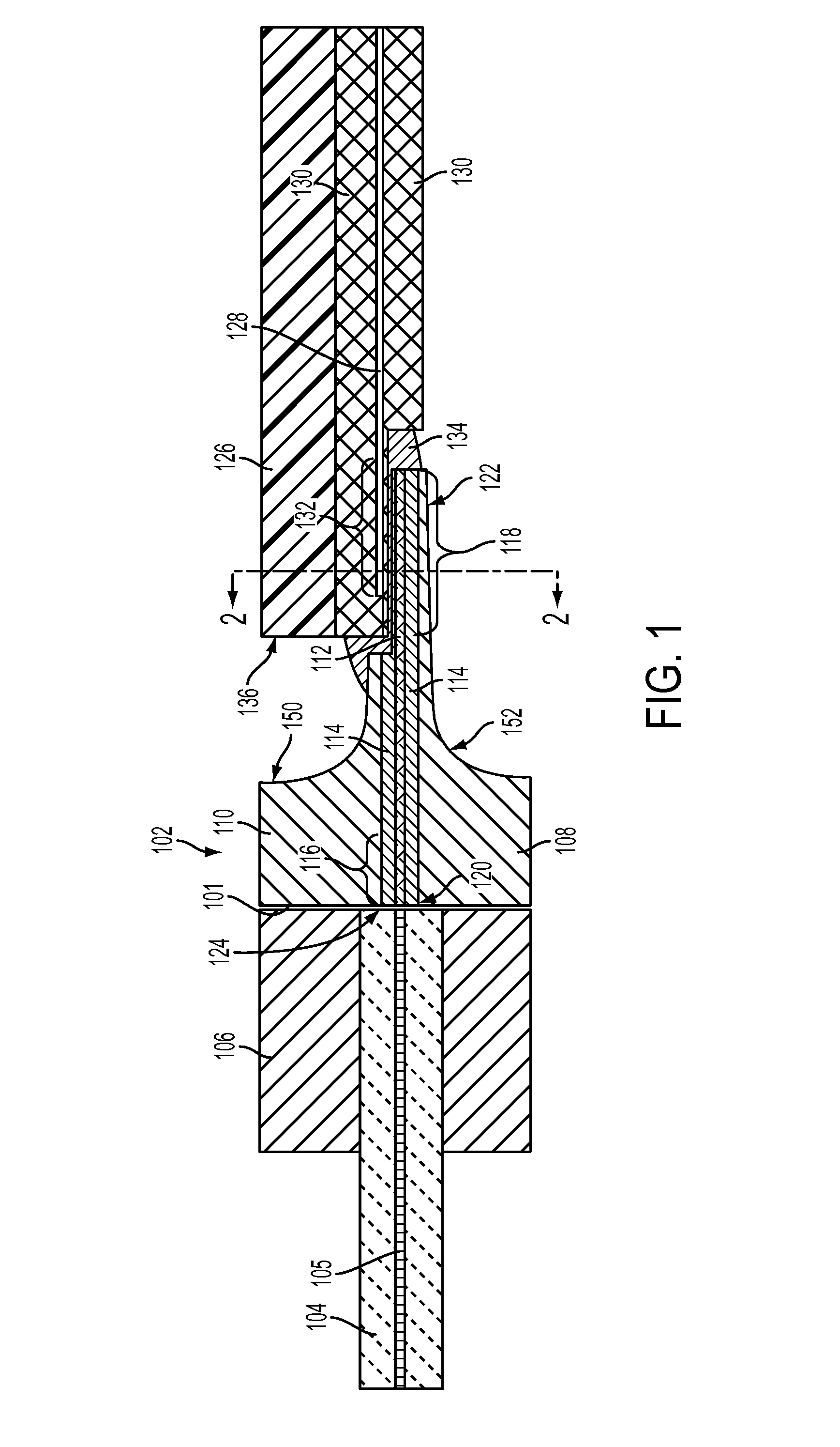
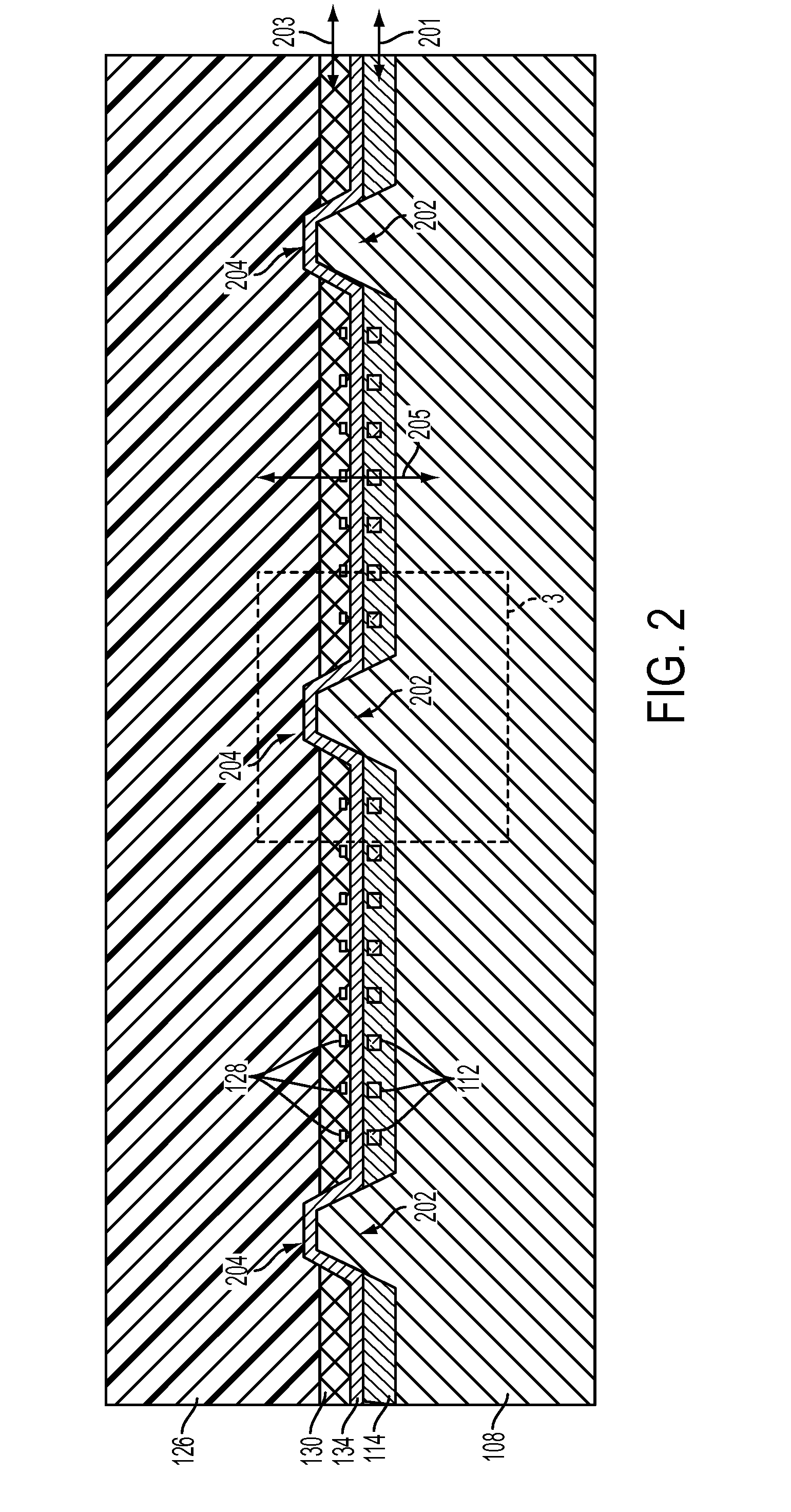
[0018]Previous interfaces between optical fiber and devices arranged on wafers were costly to manufacture. The methods and devices described below offer an economic interface for connecting optical fiber to devices arranged on wafers. In this regard, a wafer may include any type of substrate having a substantially planar surface. The wafer may include any type of suitable material or combination of materials including, for example, silicon (Si), germanium (Ge), gallium (Ga), arsenic (As), indium (In), or phosphorous (P). Any type of devices or combinations of devices may be fabricated on a wafer such as, for example, optical features, optical wave guides, mechanical features, or electronic features.

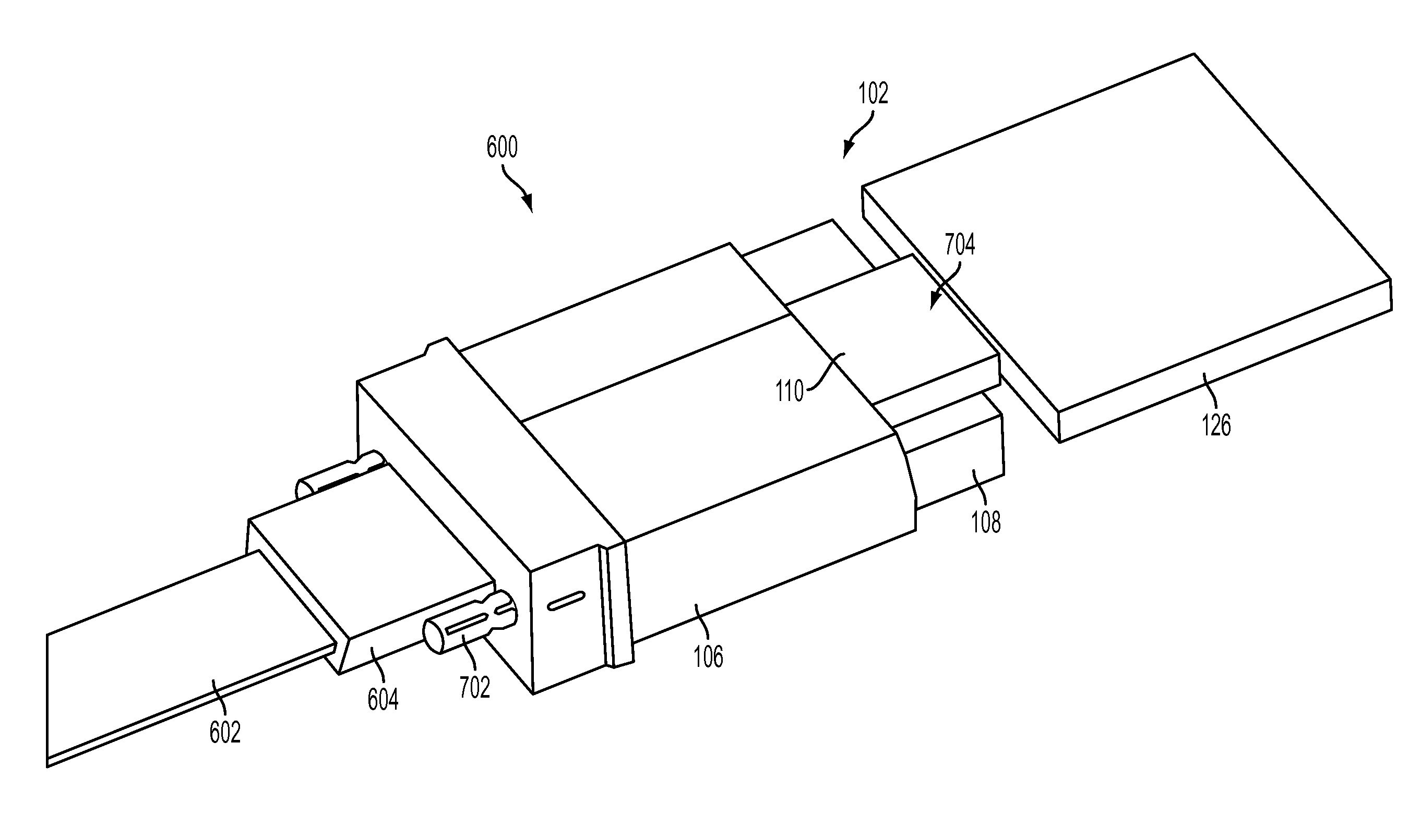
[0019]FIG. 1 illustrates a side cut-away view of an exemplary embodiment of an interface device 102. The interface device 102 is secured proximate to optical fiber(s) 104 that is arranged in an optical fiber ferrule 106. The optical fiber ferrule 106 is operative to secure at least one op...


PUM


Abstract

An interface device includes a body portion having a single-mode waveguide portion including a substantially optically transparent material, a cladding portion defined by channels contacting the waveguide portion, the cladding portion including a substantially optically transparent polymer material, an engagement feature operative to engage a portion of a wafer, and a guide portion operative to engage a portion of an optical fiber ferrule.

Description

FIELD OF INVENTION[0001]The present invention relates generally to optical signal connection devices, and more specifically, to interfaces between optical fibers and devices arranged on wafers.DESCRIPTION OF RELATED ART[0002]Optical signals may be transmitted via optical fibers. It is often desirable to connect the optical fibers to devices such as, for example, wave guides or signal processing features that may be arranged on a wafer such as, for example, a semiconductive wafer. Previous methods and devices for connecting optical devices to devices on wafers are often inefficient and costly to manufacture.BRIEF SUMMARY[0003]According to one embodiment of the present invention, an interface device includes a body portion having a single-mode waveguide portion including a substantially optically transparent material, a cladding portion defined by channels contacting the waveguide portion, the cladding portion including a substantially optically transparent polymer material, an engage...

Claims


Application Information

Patent Timeline
Patent Type & Authority Applications(United States)
IPC IPC(8): G02B6/12
CPCG02B6/30G02B6/138G02B6/125G02B6/1228
Inventor BARWICZ, TYMONCHILDERS, DARRELL R.KURTZ, DAN
Owner IBM CORP
Why Eureka
Try Eureka